The production of thick aluminum layers at moderate temperatures is of great interest for many areas of application. This article examines the electrodeposition of aluminum for printed circuit board and microsystem technology. Influencing variables on the layer morphology are presented on the basis of depositions on silicon substrates with a gold starting layer. The current density and the electrolyte temperature have a major influence on the microstructure of the layers produced. The deposition parameters evaluated for the gold starting layer cannot be transferred to an aluminum starting layer.
Vias are very important for a functional printed circuit board. Various approaches for coating such through-contacts are presented in the article. Furthermore, the structuring of the aluminum layers using photoresist including etching of the starting layer is described.
1 Introduction and motivation
The production of electrodeposited Al is technologically interesting due to the formation of a very dense, wear-resistant and corrosion-resistant Al2O3 layer. This means that steels can be protected against corrosion by the Al coating. Furthermore, the adjustable microstructure of the Al makes it possible to increase the hardness and wear resistance of the coated substrates. Due to its good electrical and thermal conductivity, low density and low price, Al can also be used in electrical engineering. Although the specific conductivity of Al is approx. 40 % lower than that of Cu, the use of Al with the same electrical and thermal conductivity, i.e. a larger cross-section, can still save 50 % in weight. Much more important than the potential weight saving when using Al is the stable world market price of Al compared to Cu. In terms of the raw material itself, Cu is approx. 2.5 to 3 times more expensive than Al. The price fluctuation of Cu in the range of 5000-7000 euros per ton is economically and politically driven. New technology trends, such as electromobility and digitalization, are increasing the demand for Cu [1]. The supply of Cu is lagging behind demand worldwide due to the increased number of strikes in Cu mines in 2017, meaning that the Cu price will continue to be subject to high fluctuations. At the 17th World Copper Conference (April 2018), public warnings were issued for the first time about dwindling copper resources. Resources are Cu mines that have already been developed and Cu ores can be mined or secondary sources from recycling. There are other Cu deposits on earth, but no mines have yet been created to extract the Cu. The construction and release of a mine usually takes several years [2].
Printed circuit board production in particular relies on pure Cu in the form of Cu foil. These foils are laminated onto the PCB substrates in order to build up the conductor pattern. However, there are only a few foil manufacturers worldwide, mainly located in Asia [3]. However, many of these copper foil manufacturers have recognized a new sales market: the battery industry. In addition, this sector has a higher turnover than the PCB industry, as thinner foils with less stringent requirements in terms of appearance and porosity are required. This has resulted in supply bottlenecks for Cu foil on the European market, which were already felt by German PCB manufacturers in 2017 [3]. It is therefore high time to develop an alternative technology to ensure the survival of the SME-driven PCB industry in Germany. The galvanic deposition of Al can provide this alternative.
In microsystems technology, Al is the standard metal for electrical cables and contact pads. Al is deposited using physical vapor deposition (PVD) processes. With this method, layers in the range of 10 nm to 2 µm can be produced. These layer thicknesses are usually sufficient for electrical cables. However, if the Al is to be used as a low-resistance lead to a thin-film resistor, an Al thickness of 10-15 µm is required. These layer thicknesses can only be achieved by electroplating.
The microsystems technology trend "More than Moore" describes the increase in integrated functionalities in an assembly. This trend is associated with 3D integration, in which the sensors and integrated circuits are built on top of each other instead of next to each other. This requires vias in the substrate (usually silicon or glass) in order to connect the components electrically and to conduct the signals to the outside. If the aspect ratio (depth/width ratio) of such holes is relatively small, PVD processes can still be used. The deeper the vias are etched into the substrate and the smaller the diameter of these holes, the more important it is to use a different coating process. Nowadays, electroplated Cu is used for this. However, coating the vias with Al would be much more attractive, as this would allow a homogeneous material system to be created. Galvanic Al deposition could therefore also be used in this area.
2 Technology
Fig. 1: Schematic representation of the deposition and decomposition process of Al for the EMImCl/AlCl3 according to [13]Electroplating is used as an established deposition method to produce the aluminum layers. A current is applied to two electrically conductive electrodes which are immersed in an electrolyte. The ions in the electrolyte are oxidized at the anode (positive pole) or, in the case of soluble anodes, formed from the elemental metal form and reduced at the cathode (negative pole). The cathode is the workpiece to be coated. The reduction of the metal ions at the cathode creates a metallic layer on the surface. Cu, Ni or Au electrolytes are usually used in assembly and connection technology (AVT). These are established processes that use water as a solvent.
Al is an electrochemically base metal with a standard potential to hydrogen (vs. NHE) of E0Al = -1.67 V. The decomposition of water depends on the pH value, but always takes place before Al reduction. Consequently, in an aqueous solution with Al ions, the decomposition of water would first occur before Al can be reduced. A different solvent is required for the separation of Al. Ionic liquids (ILs) have a broad electrochemical window and have been investigated for their suitability for use in various applications for around 30 years. These include the electrochemical deposition of metals and semiconductors [4-7], their use as electrolytes in new energy storage concepts [8, 9] or electrochemical sensors [10].
Various ILs have been investigated in the literature for electrochemical Al deposition, as different properties result depending on the composition of the IL [5]. Typical cations are 1,3-dialkylimidazolium, alkylated pyrrolidinium or ammonium ions [5, 11]. Halide ions or halide complexes (e.g. Cl-,BF4-) or more complex imides (e.g. bis(trifluoromethylsulfonyl)imide) are often used as anions [12].
For the depositions in this article, 1-ethyl-3-methylimidazolium chloride with aluminum trichloride (EMImCl/AlCl3) in a ratio of 1:1.5 from IoLiTec GmbH (Heilbronn, Germany) is used. Due to the water-binding properties of the IL, the IL is handled in a glovebox (MBraun, LABSTAR) with a dry nitrogen atmosphere (N2). The reaction mechanisms for deposition, decomposition and regeneration are shown in Figure 1.
Printed circuit boards, silicon wafers and ceramics are used as substrates. The starting layers differ depending on the substrate, but are listed below:
- Printed circuit board incl. through-contacts: Cu cladding (later Al cladding), electrically conductive polymer, graphite, Cu
- Silicon: Au and Al
Within the article, the process is scaled from small substrates (max. 2 × 5 cm²) to large substrates (150 mm diameter) and thus closer to the applications.
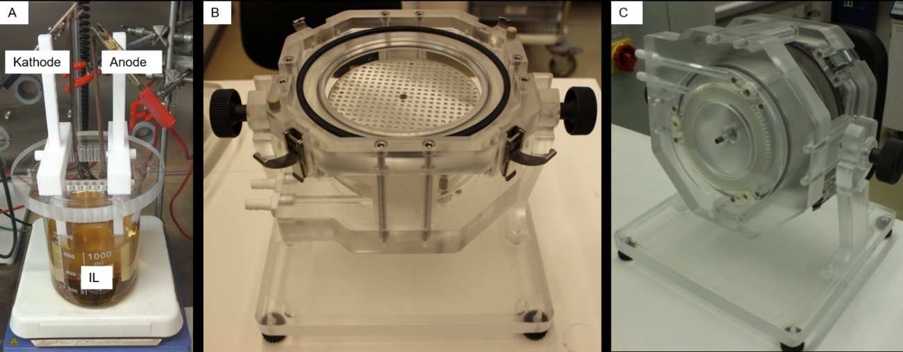
Fig. 2: A) Beaker setup for small samples, B) plating unit open, C) plating unit closed and rotated
3 Experimental framework conditions
3.1 Deposition equipment
For Al deposition at chip level, 600 ml IL is used in a beaker. The anode consists of 99.5 % pure Al and goes into solution during the deposition process, so that the IL is refreshed with Al ions (see Fig. 1). The IL can therefore be used for very long periods in a protective atmosphere. The IL is circulated moderately using a magnetic stirrer. The IL temperature is kept constant at 50 ± 2 °C.
For scaling to larger substrates, a deposition cell (plating unit) from Silicet AG is used, which is adapted to the special requirements of the ILs with regard to material compatibility. This allows wafer formats of up to 150 mm to be coated on one side. This cell can be swiveled through 180° so that the anode-cathode arrangement can be adjusted depending on the angle. The 180° position is always selected here, i.e. the sample is below the anode. The advantage of the plating unit is that only approx. 2.5 liters of electrolyte are required, even for relatively large substrates. Furthermore, the distance between the anode and cathode can be varied from a few centimetres to a few millimetres. For the following experiments, the anode-cathode distance is set at 2 cm.
Figure 2 shows the beaker set-up (A) inside the glovebox and the plating unit (B and C) outside the glovebox.
3.2 Silicon substrates
For the determination of basic deposition parameters, experiments are carried out on Si substrates with an Au starting layer (50 nm thick). Since an Au starting layer does not form an oxide layer, the deposition can be realized without pretreatment. The influence of current density and temperature on the microstructure and layer roughness is investigated. These fundamental investigations are carried out using full-surface deposition at chip level. Either 1×5 cm2 or 2×4 cm2 samples are used for this.
Since structured layers are usually used in microsystems technology, e.g. to create conductive paths or joining structures, Al deposition in photoresist structures is evaluated. Au and Al starting layers are used for this purpose. The influence of the starting layer on the layer formation behavior is explained.
Subsequently, 150 mm Si wafers are coated with Al using a resist mask for joining structures. Al and Au are also used here as the starting layer.
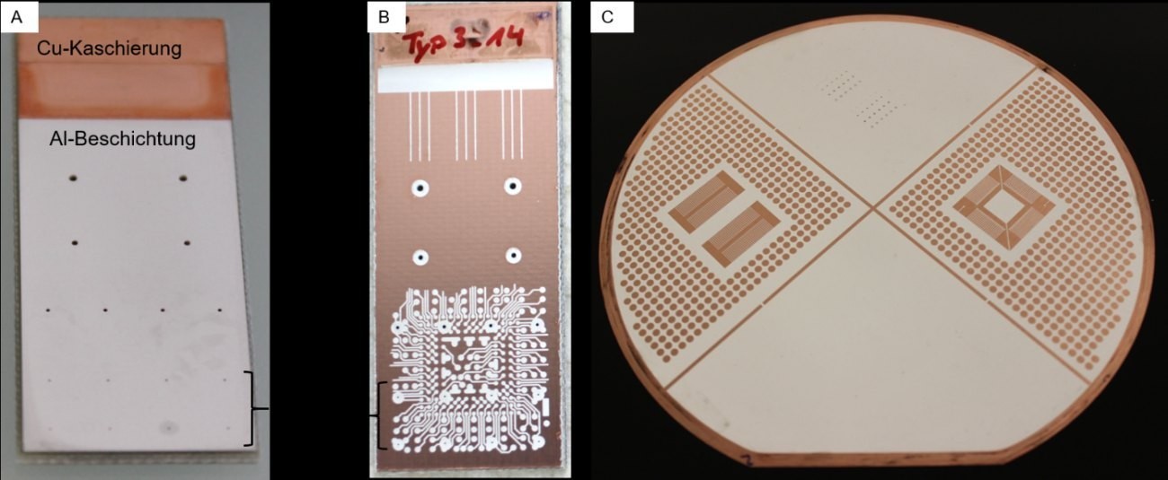
Fig. 3: Photographs of coated samples: Transmitted light sample (left), structured sample (right); the photoresist has already been removed
3.3 Printed circuit board substrates
For PCB technology, a homogeneous appearance of the coating and the realization of through-contacts are of particular interest. The through-contacts ensure the performance of a PCB with regard to two and multilayer structures. The sample types are presented in more detail below.
3.3.1 Substrate types
The coating is carried out galvanostatically in a two-electrode structure.
The deposition on the printed circuit board (PCB) substrates is carried out from both sides by placing the sample (2 × 5 cm) in the middle of two anodes (99.5 % Al). Two types of samples are used for the chip level experiments. These are shown in Figure 3. The so-called transmitted light samples are coated over their entire surface, with vias from 800 µm to 200 µm distributed over the sample (see Fig. 3 A). These samples are used to examine various starting layers in the vias (electrically conductive polymer, graphite, Cu). Furthermore, DC and pulse current depositions are compared with each other and the electrical and thermal conductivity of the Al layers are evaluated.
The second sample type is structured with photoresist (Photec 6250, MacDermidEnthone) in order to investigate the structurability of the Al (Fig. 3). Vias are also provided in the layout here. The vias are pre-coated with 1-3 µm Cu so that the feasibility of Al coating in the vias can be demonstrated on a good conductive starting layer.
The scaling of the process to PCB substrates with a diameter of 150 mm is carried out with Cu and Al lamination. The layout is the same (Fig. 3 C). Due to the microsystem equipment, only substrates in wafer format can be coated. The deposition here is one-sided. The question behind these samples is the scalability of the process and how Al deposition changes when Al lamination is used. Ultimately, the vision is an alternative technology to the Cu printed circuit board, so the lamination for building up the conductor pattern must also consist of Al.
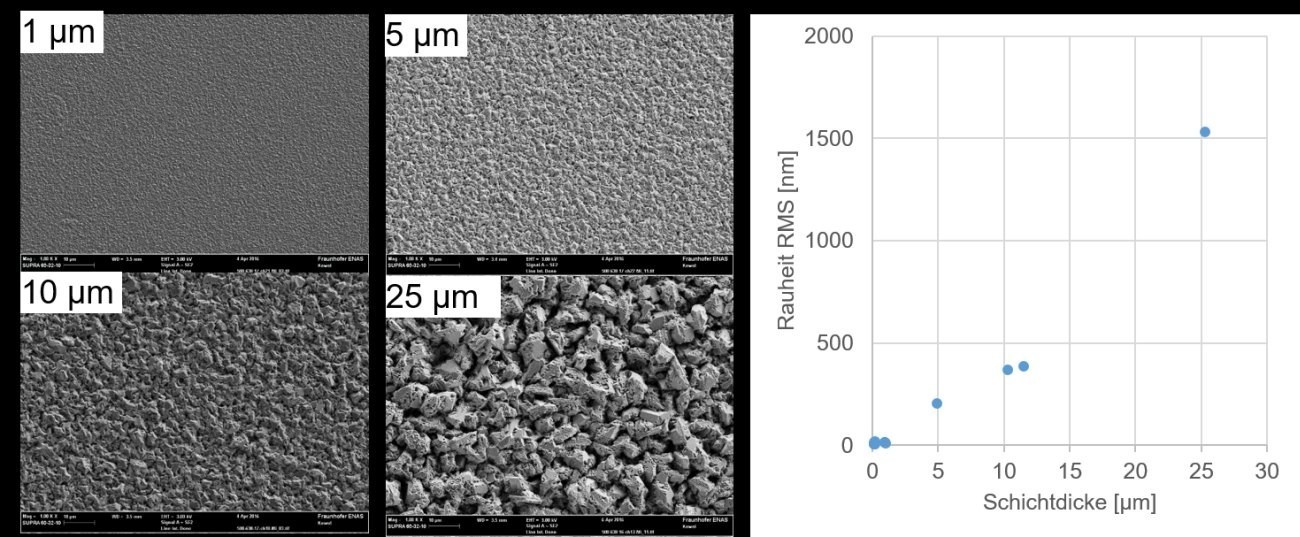
Fig. 4: Left: SEM images of the Al layers of different thicknesses; right: RMS roughness as a function of the layer thickness
3.3.2 Pre- and post-treatment
To activate the Cu surface, the samples are first pickled in a 4.5 % sodium peroxodisulphate solution (NaPS). This is followed by decapitation in 10% sulphuric acid (H2SO4). As an intermediate step, the chemicals are rinsed with deionized water (DI). Drying is carried out with a nitrogen gun.
After the coating process, the samples are thoroughly rinsed with DI water. The coating of the structured samples is removed with the resist remover PC4069 (Enthone GmbH) in 5 % dilution at approx. 40 °C. To expose the Al structures, the Cu lamination of the PCB must be selectively etched to Al. A 20 % NaPS solution is suitable for this.
No chemical pre-treatment is carried out for the Al lamination, as this must be performed outside the glovebox. The rapid re-oxidation would therefore continue to hinder the deposition. Therefore, the substrate with the Al starting layer is brought into contact with the electrolyte without pre-treatment. In the plating unit, the sample is then briefly connected as an anode to break up the oxide and release some of the Al cladding into solution. The sample is then switched to the cathode and Al deposition is started.
4 Results
4.1 Silicon substrates
4.1.1 Influence of the layer thickness on the layer roughness
The IL is used without any additives, so it can be assumed that the layer morphology changes with increasing layer thickness. Therefore, samples with 1 µm, 5 µm, 10 µm and 25 µm film thickness are deposited at 13 mA/cm2 at 30 °C. Characterization is carried out using SEM and WLI. The results are shown in Figure 4. The SEM images show that the layers with a higher layer thickness have larger grains. The roughness measurements confirm this trend. An almost linear relationship between coating thickness and roughness can be seen.
To reduce the roughness, the deposition parameters with regard to current density, IL temperature and current flow are changed in the following sections.
-to be continued-
![Abb. 1: Schematische Darstellung des Abscheide- und Zersetzungsprozesses von Al für das EMImCl/AlCl3 nach [13] Abb. 1: Schematische Darstellung des Abscheide- und Zersetzungsprozesses von Al für das EMImCl/AlCl3 nach [13]](/images/stories/Redaktion_GT/Online-Artikel/thumbnails/thumb_2020-06-Aluminium-Abscheidung01.jpg) Fig. 1: Schematic representation of the deposition and decomposition process of Al for the EMImCl/AlCl3 according to [13]Electroplating is used as an established deposition method to produce the aluminum layers. A current is applied to two electrically conductive electrodes which are immersed in an electrolyte. The ions in the electrolyte are oxidized at the anode (positive pole) or, in the case of soluble anodes, formed from the elemental metal form and reduced at the cathode (negative pole). The cathode is the workpiece to be coated. The reduction of the metal ions at the cathode creates a metallic layer on the surface. Cu, Ni or Au electrolytes are usually used in assembly and connection technology (AVT). These are established processes that use water as a solvent.
Fig. 1: Schematic representation of the deposition and decomposition process of Al for the EMImCl/AlCl3 according to [13]Electroplating is used as an established deposition method to produce the aluminum layers. A current is applied to two electrically conductive electrodes which are immersed in an electrolyte. The ions in the electrolyte are oxidized at the anode (positive pole) or, in the case of soluble anodes, formed from the elemental metal form and reduced at the cathode (negative pole). The cathode is the workpiece to be coated. The reduction of the metal ions at the cathode creates a metallic layer on the surface. Cu, Ni or Au electrolytes are usually used in assembly and connection technology (AVT). These are established processes that use water as a solvent. Fig. 2: A) Beaker setup for small samples, B) plating unit open, C) plating unit closed and rotated
 Fig. 3: Photographs of coated samples: Transmitted light sample (left), structured sample (right); the photoresist has already been removed
  Fig. 4: Left: SEM images of the Al layers of different thicknesses; right: RMS roughness as a function of the layer thickness

