The production of thick aluminum layers at moderate temperatures is of great interest for many areas of application. This article examines the electrodeposition of aluminum for printed circuit board and microsystem technology. Influencing variables on the layer morphology are presented on the basis of depositions on silicon substrates with a gold starting layer. The current density and the electrolyte temperature have a major influence on the microstructure of the layers produced. The deposition parameters evaluated for the gold starting layer cannot be transferred to an aluminum starting layer.
Vias are very important for a functional printed circuit board. Various approaches for coating such through-contacts are presented in the article. Furthermore, the structuring of the aluminum layers using photoresist including etching of the starting layer is described.
The production of thick Al layers at moderate temperatures is of great interest for many applications. In this paper the galvanic deposition of aluminum for printed circuit board and microsystem technology is investigated. Influencing variables on the layer morphology are represented by deposition on silicon substrates with a gold seed layer. The current density and the electrolyte temperature have a great influence on the microstructure of the layers produced. The deposition parameters evaluated for the gold seed layer cannot be transferred to an aluminum seed layer.
Vias are very important for a functional printed circuit board. In this article different approaches for the coating of such through-hole contacts are presented. Furthermore, the structuring of the aluminum layers is described using photoresist including etching of the seed layer.
4.2.3 Stop copper
Pulse current deposition is also investigated for the PCB samples with stop copper. This current control proved to be effective for the previous via pre-coatings. The variation of pulses with different current densities, frequencies and duty cycles was chosen in order to identify influencing variables on the coating quality.
The samples produced were characterized with regard to the following properties:
- Electrical and thermal conductivity
- Filling level of the via
Electrical and thermal conductivity
The electrical conductivity σ for Al is given in the literature as 3.6 - 10-7 S/m. With electroplated layers, such characteristic values can usually be achieved in the same order of magnitude. For the samples listed in Table 2, the electrical conductivity was determined at 25 °C, 50 °C and 100 °C using a 4-tip measurement. The thermal conductivity λ can be calculated from the σ values using Wiedemann-Franz's law. The characteristic values are listed in Table 2. Due to the manual measurement with a wafer sampling station, a measurement error of up to 20 % must be expected. In the table, the values of sample Cu31 to Cu34 are marked in green. These were measured in a batch, so that the error between them is negligible. The resulting conductivity values are very close to the values in the table for bulk Al. However, in order to make a definitive statement about the electrical and thermal conductivity of the electroplated Al, more reproducible investigations with a separate layout are necessary. With a meander structure, the distances between the measuring needles and the conductor path can be precisely maintained.
|
No. |
Current density |
Frequency |
Coating thickness |
electr. conductivity |
therm. conductivity |
||||
|
mA/cm2 |
Hz |
µm |
S/m |
W/m - K |
|||||
|
25 °C |
50 °C |
100 °C |
25 °C |
50 °C |
100 °C |
||||
|
Al |
3.6E+07 (at 20 °C) |
234 (at 20 °C) |
|||||||
|
Cu21 |
25 |
10 |
10,8 |
1,1E+08 |
7,0E+07 |
2,8E+07 |
768 |
470 |
257 |
|
Cu22 |
30 |
10 |
10,7 |
6,2E+07 |
5,9E+07 |
5,5E+07 |
451 |
417 |
504 |
|
Cu24 |
25 |
25 |
12,5 |
5,5E+07 |
5,3E+07 |
4,8E+07 |
399 |
423 |
439 |
|
Cu25 |
30 |
25 |
12,1 |
5,6E+07 |
5,4E+07 |
4,8E+07 |
409 |
404 |
436 |
|
Cu26 |
25 |
50 |
12,2 |
5,6E+07 |
5,1E+07 |
4,2E+07 |
410 |
453 |
387 |
|
Cu27 |
30 |
50 |
11,7 |
5,6E+07 |
5,7E+07 |
5,3E+07 |
406 |
379 |
481 |
|
Cu28 |
25 |
25 |
19,1 |
4,8E+07 |
4,8E+07 |
4,4E+07 |
353 |
442 |
400 |
|
Cu29 |
30 |
25 |
16,6 |
5,1E+07 |
5,6E+07 |
5,8E+07 |
376 |
420 |
526 |
|
Cu30 |
25 |
50 |
15,1 |
6,0E+07 |
5,3E+07 |
5,3E+07 |
441 |
248 |
486 |
|
Cu31 |
30 |
25 |
17,4 |
3,4E+07 |
3,1E+07 |
2,9E+07 |
246 |
234 |
261 |
|
Cu32 |
30 |
25 |
17,7 |
3,2E+07 |
3,0E+07 |
2,7E+07 |
231 |
248 |
245 |
|
Cu33 |
30 |
25 |
16,2 |
3,4E+07 |
3,1E+07 |
3,1E+07 |
247 |
235 |
280 |
|
Cu34 |
21 |
- |
17,8 |
3,2E+07 |
3,0E+07 |
2,8E+07 |
231 |
235 |
256 |
Fill level of the vias
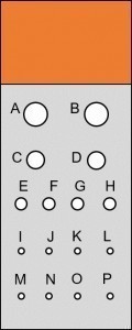
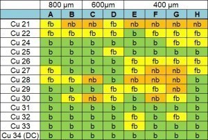
To determine the degree of filling, the vias with a diameter of 800 µm and 600 µm were arranged on an incline under an optical microscope. These via sizes can be reliably estimated using this method. The 400 µm and 200 µm vias, on the other hand, must be prepared by cross-sectioning. A marking was introduced for the assignment of the vias on the samples (see Fig. 11). The vias are characterized as "coated (b)", "almost coated (fb)" and "not coated (nb)". Here, fb means that the Cu still shines through the Al layer to some extent. With nb, the Cu is still clearly visible. Figure 12 shows the evaluation of the via diameters 800-400 µm. It can be seen that the samples with lower layer thicknesses (up to Cu27) are often grouped with "fb". Sample Cu25 stands out here: almost all vias are categorized as "coated". Samples Cu31-33 were also coated with the deposition parameters of Cu25, whereby these repeat samples were charged twice (twice the current, same time). A good coating up to 400 µm via could also be determined for these samples. Subsequent cross-sectional examinations of the 400 µm and 200 µm vias should make it possible to draw meaningful conclusions.
Figure 13 shows optical microscope images of the 400 µm "F" and "G" vias of samples Cu31 to 33. The "F" vias are fully coated. The "G" vias, on the other hand, are not completely coated with Al. In the case of the "G" vias, it is clear that Al clusters (marked in red) have formed at the corners of the via openings, which are always exactly opposite the area with exposed Cu. This behavior is frequently observed in the investigations. One possible explanation for the open Cu spots is the poor via flow in the beaker, so that gas bubbles are trapped on the via walls. The edges of the via openings have a locally higher current density, so that Al ions flowing out of the via discharge faster there and thus accumulate these clusters. This effect can also be observed in aqueous systems if no additives with a suppressing effect (suppressor) are used.
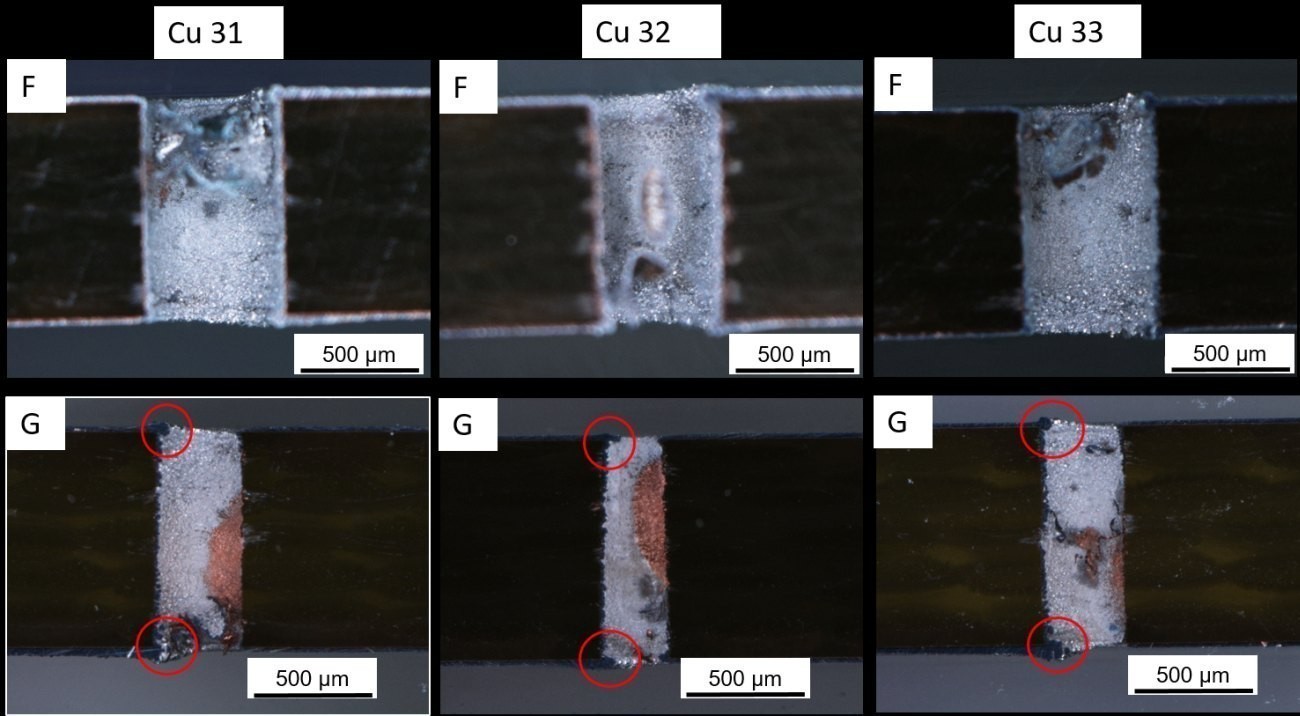 Fig. 13: Light microscope images of 400 µm via "F" and "G" of samples Cu31-33
The filling level of the 200 µm vias is shown in Figure 14 as an example for "K" and "O". The "O" vias are completely coated for all samples. In the "K" vias, however, the Cu starting layer still shines through the Al layer. The Al layer is not yet completely built up. Nevertheless, the vias are coated with Al from top to bottom. In summary, the coating of via sidewalls with a Cu starter layer can be demonstrated in a simple test setup. Although the homogeneity across a sample poses further challenges. The vias at the edges of the sample are always more heavily coated than the vias in the center of the sample. Cathode movement between the anodes, as is common in the PCB industry, does not show any significant improvement in the beaker structure.
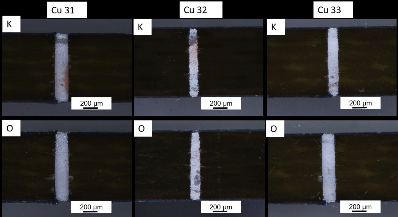 Fig. 14: Light microscope images of 200 µm via "K" and "O" of samples Cu31-33
4.2.4 Structuring of the Al layers
Figure 15 shows the process chain for patterned Al deposition, with the white structures being the Al layer. In Figure 15 A, the sample is coated with the resist "Photec 6250". This is removed with the resist remover PC4069. The underlying Cu, which serves as the starting layer for the deposition, is exposed with a 20 % NaPS solution (see Fig.15 B). The Al structures are exposed by etching the Cu(Fig.15 C).
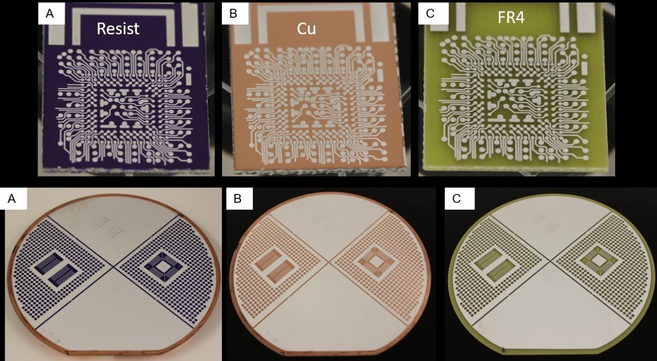 Fig. 15: Photographs of the process sequence for the production of structured Al layers on Cu lamination for chip and wafer format
The transfer of the deposition and the release of the structures must also be transferable to larger substrates. Therefore, the depositions on 150 mm wafer format were not examined with regard to the microstructure, but for further process capability. The deposition on Cu and Al lamination is carried out by means of pulsed current deposition. The homogeneity and density of the layers has been proven from the chip level investigations. Adhesion tests have been carried out for the Al lamination to ensure that the anodic return pulse for oxide removal is sufficiently long.
The resist is removed equally with the PC4069 for Al and Cu lamination. With Cu lamination, the structuring process can be transferred one-to-one from Chiplevel(Fig. 15). However, the etchant for releasing the Al structures on Al cladding is not trivial, as the attack is equally strong everywhere. However, the use of alkaline etching solutions appears to be more promising than acidic etching solutions.
5 Summary and outlook
Electroplated Al deposition was investigated with regard to the influencing factors of current density, temperature, current conduction and starting layer on Si substrates. The results show that higher current densities have a positive effect on layer formation during Al deposition. Furthermore, it is advantageous to work at higher temperatures, as the deposition rate increases due to the increased ion mobility. For coatings produced with current densities > 20 mA/cm2, the temperature influence from 30 °C to 50 °C is small. The microstructure hardly changes as the crystallization potential is sufficiently high. Pulsed current deposition provides further variables in the deposition process. The duty cycle appears to be decisive. If the pulse pause is too long, the average current density decreases and thus the layer roughness increases. The deposition parameters of the chip level investigations could be transferred to wafer level. However, Au as a starting layer behaves differently to Al, so that the optimum deposition parameters for an Al starting layer still need to be evaluated.
On the PCB substrates, the coating of vias with different starting layers is being considered. The basic feasibility of via coating can be successfully demonstrated with Cu pre-coated vias, although the homogeneity of the coating across the sample cannot be guaranteed. For a complete Al printed circuit board, however, deposition on the electrically conductive polymer or graphite layer would be desirable. The approaches for this are promising. However, further research work needs to be invested in the electrolyte and the system technology in order to realize this. The electrolyte must have a higher conductivity and the electrolyte should flow directly through the vias to ensure ion exchange. The electrical and thermal conductivity of the Al layers is comparable to pure Al. As the measurement method used here is not sufficiently stable, the layers should be measured again using a separate layout. In this layout, the Al layer is structured using pattern plating. This method can be used for the copper cladding of the PCB. Al lamination is more complex in terms of structure release, as both the lamination and the galvanic layer are equally attacked by an etching medium.
The investigations lay the foundation for further research and development work in the field of Al deposition for microsystem and PCB technology. An alternative technology to the previous copper printed circuit board is of particular interest to the printed circuit board industry. In order to bring Al deposition to industrial maturity, further research is needed into the electrolyte, the plant technology, the recycling of the electrolyte and the deposition behavior when the composition of the electrolyte changes.
Acknowledgments
The authors would like to thank the Federal Ministry of Education and Research for funding within the "KMU-innovativ für die Informations- und Kommunikationstechnologie" initiative (project "AioLi", funding code 16ES0329K). The authors would also like to thank the project partners First Sensor Microelectronic Packaging Dresden GmbH, Jenaer Leiterplatten GmbH, IoLiTec GmbH, Smart Membranes GmbH, Siegert Thinfilm Technology GmbH and NB Technologies GmbH for their continued excellent cooperation.
References
- G. Angerer; A. Mohring; F. Marscheider-Weidemann; M. Wietschel: Copper for future technologies, (2010)
- https://www.elektronikpraxis.vogel.de/knappes-kupfer-bis-2035-schliessen-weltweit-200-minen-a-704986/ Status: 12.04.2018
- https://www.elektronikpraxis.vogel.de/engpass-kupferfolie-wohin-driftet-die-leiterplattenindustrie-a-579650/index2.html/ As at: 30.12.2017
- P.-Y. Chen; I.-W. Sun: Electrochemical study of copper in a basic 1-ethyl-3-methylimidazolium tetrafluoroborate room temperature molten salt, Electrochimica Acta, 45 (1999) 441-450
- F. Endres; Bukowski; R. Hempelmann; H. Natter: Electrodeposition of nanocrystalline metals and alloys from ionic liquids, Angewandte Chemie, International Edition, 42 (2003) 3428-3430
- S.Z. El Abedin; A.Y. Saad; H.K. Farag; N. Borisenko; Q.X. Liu; F. Endres: Electrodeposition of selenium, indium and copper in an air- and water-stable ionic liquid at variable temperatures, Electrochimica Acta, 52 (2007) 2746-2754
- M.K. Carpenter; M.W. Verbrugge: Electrochemical codeposition of gallium and arsenicfrom a room temperature chlorogallate melt, Journal of the Electrochemical Society, 137 (1990) 123-129
- M. Armand; F. Endres; D.R. MacFarlane; H. Ohno; B. Scrosati: Ionic-liquid materials for the electrochemical challenges of the future, Nature Materials, Vol. 8(2009) 621-629
- D.R. MacFarlane et al: Energy applications of ionic liquids, Energy&Enviromental Science, 7 (2014) 232-250
- F. Faridbod; M.R. Ganjali; P. Norouzi; S. Riahi; H. Rashedi: Application of Room Temperature Ionic Liquids in Electrochemical Sensors and Biosensors, Ionic Liquids: Applications and Perspectives, Prof. Alexander Kokorin (Ed.), (2011)
- M. Galinski; A. Lewandowski; I. Stepniak: Ionic liquids as electrolytes, Electrochim. Acta, vol. 51, no. 26, (2006) 5567-5580
- F. Endres; D. MacFarlane; A. Abbott, Eds: Electrodeposition from Ionic Liquids, Wiley-YCH, (2008)
- E. Berretti et al: Aluminum electrodeposition from ionic liquid: Effect of deposition temperature and sonication, Materials (Basel), Vol. 9, no. 9, (2016) 1-14
- Devaraj: Pulse plating, Materials Chemistry and Physics, 25 (1990) 439-461
- B. Li; C. Fan; Y. Chen; J. Lou; L. Yan: Pulse current electrodeposition of al from an AlCl3 -EMIC ionic liquid, Electrochimica Acta, 56, (2011) 5478-5482
- J. Tang; K. Azumi: Optimization of pulsed electrodeposition of aluminum from alcl3-1-ethyl-3-methylimidazolium chloride ionic liquid, Electrochimica Acta, 56, (2011) 1130-1137
- N. Kanani: Galvanotechnik - Grundlagen, Verfahren, Praxis, Carl Hanser Verlag, Munich, Vienna, (2000)


