- Part 1 - Phenomena, phase formation, diffusion processes
Tin whiskers are spontaneously growing, mostly monocrystalline filaments with a diameter of a few μm and a length of up to several mm. They are mainly formed on electroplated tin-plated copper substrates, which is the predominant technology used in the assembly of integrated circuits. Due to their dimensions, whiskers pose a serious problem for the reliability of such components because, as a result of the miniaturization of electronics, they are so large that they can cause short circuits and failures of entire devices. The article, which is continued in a second part, shows that the relationship between crystal recovery processes and intermetallic phase formation determines whisker growth.
For a long time, the addition of lead proved to be an effective means of reducing whiskers to a negligible level. However, the ban on lead in electronic components enforced by European legislation led to a dramatic reawakening of the whisker problem [1-3]. This paper puts older work into context to help fill gaps in our understanding of the growth mechanism [4-8].
Whiskers - a pressure release phenomenon
Since their first description in the scientific literature, whiskers in general [9] and tin whiskers in particular [10, 11] have resisted a widely accepted explanation regarding a growth mechanism, [12, 13] although experts agree on "how" whiskers grow. However, they have not yet been able to answer "why", or only partially, and therefore continue to refer to the process as "spontaneous". The most important prerequisite for whisker growth is the formation of pressure on or compressive stress within the tin layer, [11] whereby this can be externally applied pressure, [14] pressure due to different thermal expansion of the coated material compared to tin [15], and pressure due to strong oxide formation [16]. From a practical point of view, however, by far the most important is the pressure that forms due to intermetallic phase formation, especially in the case of tinned copper and copper alloy substrates [17].
Intermetallic phase formation as the main cause of pressure
The intermetallic phase (intermetallic compound, IMC) Cu6Sn5 forms within the tin layer, as copper diffuses unidirectionally into tin [18].This IMC growth can be very well documented by selective etching of the tin layer (Fig. 1) [5, 6]. The Cu6Sn5 crystal formation is already clearly visible half an hour after coating the copper substrate, after 15 hours some pyramidal crystals are already larger than 1 μm and after just under a week individual crystals exceed a value of 2.5 μm. It is striking that the vast majority of Cu6Sn5 crystals line up along the grain boundaries of the etched tin layer, but also how different in size these crystals are. Regardless of this, it is obvious that the additional space taken up by these crystals must be accompanied by an increase in pressure within the tin layer.
![Abb. 1: Intermetallische Phasenbildung in Abhängigkeit der Inkubationszeit nach selektivem Abätzen der Zinnschicht (AFM-Bilder im Tapping-Modus, 10 µm Kantenlänge (aus [6])](/images/stories/Abo-2023-09/gt-2023-09-061.jpg) Fig. 1: Intermetallic phase formation as a function of the incubation time after selective etching of the tin layer (AFM images in tapping mode, 10 µm edge length (from [6])
Fig. 1: Intermetallic phase formation as a function of the incubation time after selective etching of the tin layer (AFM images in tapping mode, 10 µm edge length (from [6])
Discrepancy to IMC-induced whisker growth
However, this is where the problems in formulating a coherent growth mechanism begin. While a clear dependence of the number of whiskers on the pressure or the distance to the clamp can be observed when pressure is applied externally with clamps [14], such a dependence does not appear to exist for IMC-induced ![Abb. 2: Durch IMC-Bildung resultierende Gewichtszunahme verschiedener Kupfersubstrate in Abhängigkeit der Inkubationszeit nach selektivem Abätzen der Zinnschicht (aus [6])](/images/stories/Abo-2023-09/thumbnails/thumb_gt-2023-09-062.jpg) Fig. 2: Weight increase of various copper substrates resulting from IMC formation as a function of the incubation time after selective etching of the tin layer (from [6]) whiskers. As an example, the difference between the two copper base materials commonly used in electronics, C19400 and C70250, should be noted, which have a very different influence on the whisker growth behavior of the tin layers applied to them. For example, tin-coated C19400 substrates exhibit a significantly higher occurrence of whiskers than their counterparts made of C70250. This fact, which is astonishing in itself, is all the more astonishing because almost twice as much of the predominant intermetallic phase Cu6Sn5 is formed in C70250-coated parts compared to C19400 (Fig. 2), which is in striking contradiction to the statement that IMC formation causes whisker growth [6]. The fact that the two substrates exhibit such different IMC growth rates is due to the different preferred copper orientations, (100) for C19400 and (110) for C70250. The resulting different packing densities on the copper surface lead to lower activation energies in the case of C70250 and thus higher mobilization of copper atoms than is the case for C19400 [19]. Copper single crystals were also coated in order to exclude any influences of alloying elements (Fe, Zn and P for C19400, Ni, Mg and Si for C70250). Both the IMC and the whisker growth behavior were almost identical to the results with the industrially used copper substrates: Almost twice as high IMC formation with both C70250 and Cu(110) compared to C19400 and Cu(100). And accordingly, practically no whiskers grew on the former, while massive whisker growth was observed on the latter [6]. Nevertheless, it must be assumed that Cu6Sn5 formation is of central importance for the formation of whiskers, since no whiskers are observed in its complete absence under normal conditions. Consequently, there must be other influences that significantly affect whisker growth.
Fig. 2: Weight increase of various copper substrates resulting from IMC formation as a function of the incubation time after selective etching of the tin layer (from [6]) whiskers. As an example, the difference between the two copper base materials commonly used in electronics, C19400 and C70250, should be noted, which have a very different influence on the whisker growth behavior of the tin layers applied to them. For example, tin-coated C19400 substrates exhibit a significantly higher occurrence of whiskers than their counterparts made of C70250. This fact, which is astonishing in itself, is all the more astonishing because almost twice as much of the predominant intermetallic phase Cu6Sn5 is formed in C70250-coated parts compared to C19400 (Fig. 2), which is in striking contradiction to the statement that IMC formation causes whisker growth [6]. The fact that the two substrates exhibit such different IMC growth rates is due to the different preferred copper orientations, (100) for C19400 and (110) for C70250. The resulting different packing densities on the copper surface lead to lower activation energies in the case of C70250 and thus higher mobilization of copper atoms than is the case for C19400 [19]. Copper single crystals were also coated in order to exclude any influences of alloying elements (Fe, Zn and P for C19400, Ni, Mg and Si for C70250). Both the IMC and the whisker growth behavior were almost identical to the results with the industrially used copper substrates: Almost twice as high IMC formation with both C70250 and Cu(110) compared to C19400 and Cu(100). And accordingly, practically no whiskers grew on the former, while massive whisker growth was observed on the latter [6]. Nevertheless, it must be assumed that Cu6Sn5 formation is of central importance for the formation of whiskers, since no whiskers are observed in its complete absence under normal conditions. Consequently, there must be other influences that significantly affect whisker growth.
Strongly localized pressure relief leads to whiskers
One of these possible factors is the rapidly forming oxide layer on the tin surface, which prevents the pressure from being reduced ubiquitously by tin self-diffusion and instead builds up continuously in the layer. The pressure slowly increases until the oxide layer is broken through at its weakest point and, highly localized, marks the beginning of whisker growth (Fig. 3). This theory, which has become known as the 'cracked oxide theory' (COT) [20, 21], has not yet been conclusively confirmed experimentally. However, it takes up a motif that was formulated very early in the scientific literature, namely that whisker growth occurs when general diffusion pathways have been restricted or completely prevented [22]. This argument was first verified in mechanically pressurized aluminum platelets with tin inclusions [23, 24]. [23, 24].
Tracer experiments with the radionuclide 113Sn(electron capture, 1036 keV, T1/2 115.09 days) are particularly illustrative [25]. Here, the tracer was applied to a glass plate, which was then coated with inactive tin from the vapor phase at 5*10-7 Torr (1 Torr ≈ 133.322 Pa) and aged at 60 °C. A proportional counter tube was used to measure a continuous increase in radioactivity, which can be explained by the fact that the relatively low-energy radiation generated from conversion electrons during electron capture, which was initially absorbed by the inactive tin, now moved towards the surface by diffusion and could be increasingly detected. This changed abruptly when the deposition was not carried out in a high vacuum, but at an oxygen pressure of 10-4 Torr. Over the entire observation period of 80 hours, no increase in radioactivity could be detected, which indicates that the oxygen contamination impaired the structure to such an extent that almost no continuous diffusion was possible. However, a large number of whiskers formed during aging, which were themselves radioactive and thus represent a hardly refutable indication for the thesis of strongly localized stress reduction. However, the results also contradict the COT, because if only the breakthrough of the surface oxide layer was responsible for the local pressure reduction, an increase in radioactivity, albeit reduced, should have been observed. The absence of such an increase implies that the homogeneous diffusion of the tracer was prevented very early on within the tin layer.![Abb. 3: Schematische Darstellung der ‚Cracked Oxide Theory‘ (aus [21]) gt 2023 09 063](/images/stories/Abo-2023-09/thumbnails/thumb_gt-2023-09-063.jpg) Fig. 3: Schematic representation of the 'cracked oxide theory' (from [21])
Fig. 3: Schematic representation of the 'cracked oxide theory' (from [21])
Grain boundaries as the site of action
Obviously, impurities seem to have a decisive influence on the tendency of a tin layer to form whiskers - both positively and negatively. For example, there are extensive studies that prove that copper in low concentrations promotes very strong whisker growth [26]. Others suspect an influence of carbon in the coating and refer to the general tendency of bright tin to form more whiskers than matt tin [13]. Lead, but also other alloy components such as silver and nickel, are able to suppress whisker growth to such an extent that it is no longer a cause for concern from a technical point of view [27-29]. What all these reports have in common is that the impurities are deposited in the grain boundaries and thus influence whisker growth. Conversely, this means that the grain boundaries of the tin layer determine whether whiskers grow or not and to go one step further, it is especially the diffusion behavior along the grain boundaries that is crucial. In fact, grain boundary diffusion (DGB) is the predominant type of diffusion in solids. Compared to diffusion in the crystal lattice (DV, volume diffusion), it is generally faster than the latter by a factor of 104 to 108 (!) due to the fact that the activation energy is only about half as high [30]. On the one hand, this fact is expressed very clearly in the IMC formation described above. On the other hand, it can be assumed that not only the copper-in-tin diffusion, but also the tin self-diffusion takes place distinctly along the grain boundaries. The decisive factor is that the grain boundary structure is not only influenced by foreign atoms, but first and foremost by the spatial arrangement of neighboring tin crystals, which create the intervening grain boundary in the first place.
Texture of the tin layer defines grain boundaries
An electroplated layer is the result of electrocrystallization and as such is produced in an electric field. Naturally, such crystals do not grow stochastically in all directions, but are oriented along the electric field lines present during deposition. Consequently, the deposited layer has a pronounced preferred orientation, also known as texture, which means, among other things, that the crystal planes of neighboring crystals are more or less aligned. In this idealized view, the adjacent crystals fit together so perfectly that the grain boundaries disappear.
However, the orientation along the electric field lines has a second, obvious consequence, namely that the crystals grow vertically to the substrate, which means that most electroplated layers have a so-called columnar structure. This means that during electrocrystallization, at least at the time of nucleation, one degree of freedom remains, namely the rotation of the columns around their own axis. In fact, up to a layer thickness of about 0.2 µm, no formation of a preferred orientation is observed. Instead, pebble-like islands form, which spread laterally in a caterpillar shape until a closed layer has formed. Only then does height growth begin, which at first appears as if icing has been poured over the pebbles (Fig. 4) [31]. Obviously, the substrate must first be covered with a closed layer before an orderly layer build-up can take place, which is also characterized by the fact that a defined texture with easily recognizable grain boundaries now forms. This layer growth in turn is largely determined by the deposition conditions and the organics in the electrolyte.
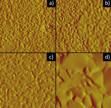 Fig. 4: AFM images in tapping mode (edge length of the images 10 µm) of nominal 0.06 (4a), 0.12 (4b), 0.25 (4c) and 5 (4d) µm thick tin layers
The latter suppresses the development of hydrogen in acidic electrolytes, which is a prerequisite for a usable layer. Secondly, however, there is a suppression of the tin deposition, which manifests itself in the fact that the electrocrystallization within a single grain no longer takes place along the electric field lines but, depending on the strength of the suppression, more or less tilted to these field lines, resulting in the textures observable by X-ray diffraction. The tilted growth axis is observed equally in all grains, which is important because the angle of inclination Φ of the crystal planes (also interplanar angle) defines the dimension of the grain boundary between two neighboring grains. A tilt of Φ less than 15° is referred to as a small angle grain boundary (GBsa) and Φ greater than 15° as a large angle grain boundary (GBla) [30]. Corresponding to the much larger number of defects, the diffusion rate in the case of GBla is orders of magnitude faster than for GBsa, which in turn approaches values of volume diffusion. As already mentioned, these different diffusion rates can be illustrated very nicely using the IMC morphology in Figure 1, which should also apply analogously to tin self-diffusion.
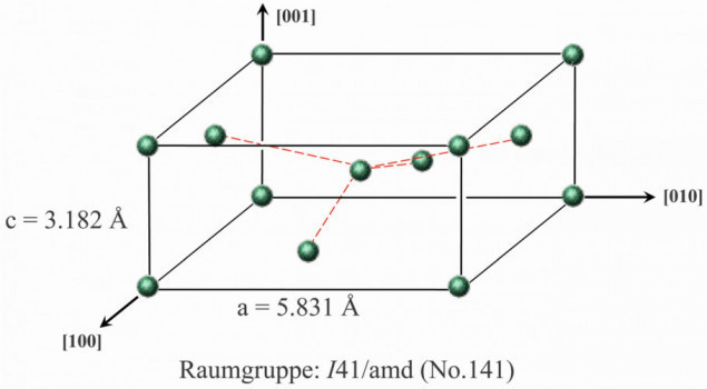
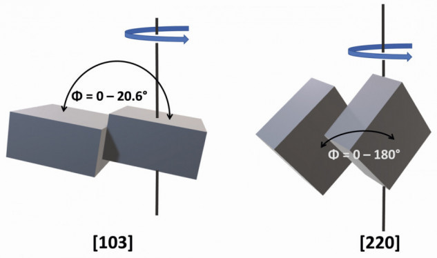
If we now consider two hypothetical cases of tin electrocrystallization with different suppression, we can quickly see that the texture of the tin layer has a major influence on the dimension of the grain boundaries. For this purpose, one should first have a rudimentary idea of the space-centered tetragonal β-tin crystal lattice (space group no. 141). By definition, only 90° angles are present. The edge lengths are a = b = 3.182 Å and c = 5.831 Å (Fig. 5). If you now want to describe the texture of a layer, this is generally done using the so-called Miller indices "hkl", where h corresponds to the axis section in the crystal lattice in the x-direction, k in the y-direction and l in the z-direction. As an example, a (103) and a (220) texture are compared with each other. If a (103)-oriented grain is fixed and a neighboring (103) grain is rotated around its z-axis, it can be seen that the angle of inclination Φ between the crystal planes moves in a narrow range between 0° and 20.6° (Fig. 6). In other words, a tin layer with a (103) texture forms practically exclusively small-angle grain boundaries.
A completely different picture emerges from the same observation of a (220)-oriented tin layer. Now the values for Φ oscillate between 0° and 180°, which results in the formation of predominantly large-angle grain boundaries. In other words, it is the texture that determines the extent to which grain boundary diffusion can take place. Derived from this and combined with the statement that whisker growth occurs when general diffusion paths are restricted, the hypothesis arises that tin layers containing predominantly small-angle grain boundaries tend to exhibit significantly stronger whisker growth than those with large-angle grain boundaries (Critical Angle Theory, CAT) [4, 32].
Diffusion processes within the tin layer
Theoretically, it should be possible to visualize grain boundary diffusion experimentally. In fact, there are countless SEM images of top views and cross-sections (mechanical and using focused ion beam, FIB), which document the grain structure, the tin layer structure and the distribution of intermetallic phases in it very well, but from which no information about the diffusion behavior of tin emerges [26]. Instead, the tin layer appears to be an absolutely rigid structure that does not seem to change at all. However, one should be aware that, on the one hand, the superficial oxide layer makes it impossible to observe structural changes in the tin layer and, on the other hand, the tin layer can hardly be mechanically processed without either smearing structures or applying so much thermal energy that the features then described have hardly anything to do with the original state of the layer.
These difficulties can be elegantly circumvented by etching the tin layer with an alkaline ortho-nitrophenol solution. Of course, this process also changes the tin layer. In contrast to the mechanical processing methods, however, etching is a chemical process and corresponds to the tin layer in that areas with a high density of imperfections dissolve much faster than flawless areas, resulting in an image that at least partially allows the tin self-diffusion paths to be visualized. With an etching speed of around 0.3 µm/s on average, 10 µm thick tin layers can be completely etched off in a controlled manner in just over 30 seconds.
Subsequently, various C19400 substrates coated with 10 µm tin were etched for different lengths of time immediately after coating (10 to 15 seconds delay due to rinsing) (Fig. 7). The applied silky-glossy tin layer was characterized by a (211)(321) texture, which corresponds to very common preferred orientations of matt tin processes and in which a large proportion of small-angle grain boundaries are formed. After two seconds of etching, polygonal etch pits are formed (Fig. 7a), which are characteristic of underlying screw dislocations [33]. It is interesting to note that there are several such etching pits within one grain, meaning that one grain has grown by means of several screw dislocations. This impression is reinforced as the etching time progresses: after 10 seconds, most of the etching pits have disappeared (Fig. 7b). In their place, however, a fine-fibrous, furry morphology has emerged, which suggests that a grain consists of hundreds, if not almost thousands, of fascicularly arranged fibers, which most likely result from an equally large number of screw dislocations. These screw dislocations in turn appear to organize themselves within a grain to form a superordinate super-screw dislocation (inset Fig. 7c) [34].
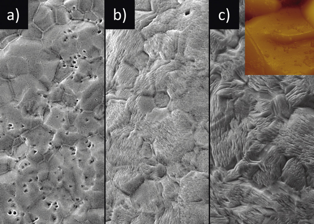 Fig. 7: SEM images (5000x magnification) at a) 2 seconds b) 10 seconds and c) 15 seconds etching time for a (221)(321)-oriented tin layer
After a further 5 seconds (15 seconds in total) etching time, the fiber-like structure is even more pronounced and coarser than after 10 seconds. Obviously, recrystallization already takes place within the tin layer during coating, which is not surprising due to the low melting temperature of the tin of 232 °C and the resulting high homologous temperatureTH of just under 0.6 at room temperature. In other words, what is perceived as an immovable grain in the unetched state is in fact a conglomerate of subcrystalline structures that are also characterized by extremely dynamic diffusion behaviour. But how can this finding be transferred to whisker growth?
To answer this question, the etching experiment was repeated with samples aged for six days, a period of time that roughly corresponds to the latency period after which the first whiskers usually appear at the latest. This test revealed the full extent of the dynamics within the tin layer. A comparison of the freshly deposited layers etched for 15 seconds on the one hand and aged layers on the other (Fig. 8) reveals that the recrystallization of the tin fibres, which could perhaps best be described as coalescence of the fibres, takes place across all grains with increasing age. While the coalescence of the fibers initially takes place within the boundaries of what can be described as grain, and thus corresponds to a certain extent to the grain structures observable from the surface (Fig. 8b), this correspondence of the surface (Fig. 8a and 8c) with the underlying layered structure is no longer present in aged samples (Fig. 8d). The grains and thus also the grain boundaries have largely disappeared and thus naturally also grain boundary diffusion. This means that vertical diffusion along grain boundaries is increasingly suppressed within the investigated time span of six days, until the tin layer is presumably completely sealed horizontally. This provides the conditions for a continuous pressure build-up with subsequent whisker growth. In contrast to the 'cracked oxide theory', the suppression of grain boundary diffusion through the annihilation of these very grain boundaries is much more profound, which can now be reconciled with the above-mentioned tracer experiments without contradiction. However, this does not yet answer the question of the influence of the speed of IMC formation. Neither does it answer many other questions, such as the well-known observation that different tin coating processes have very different tendencies to whisker formation.
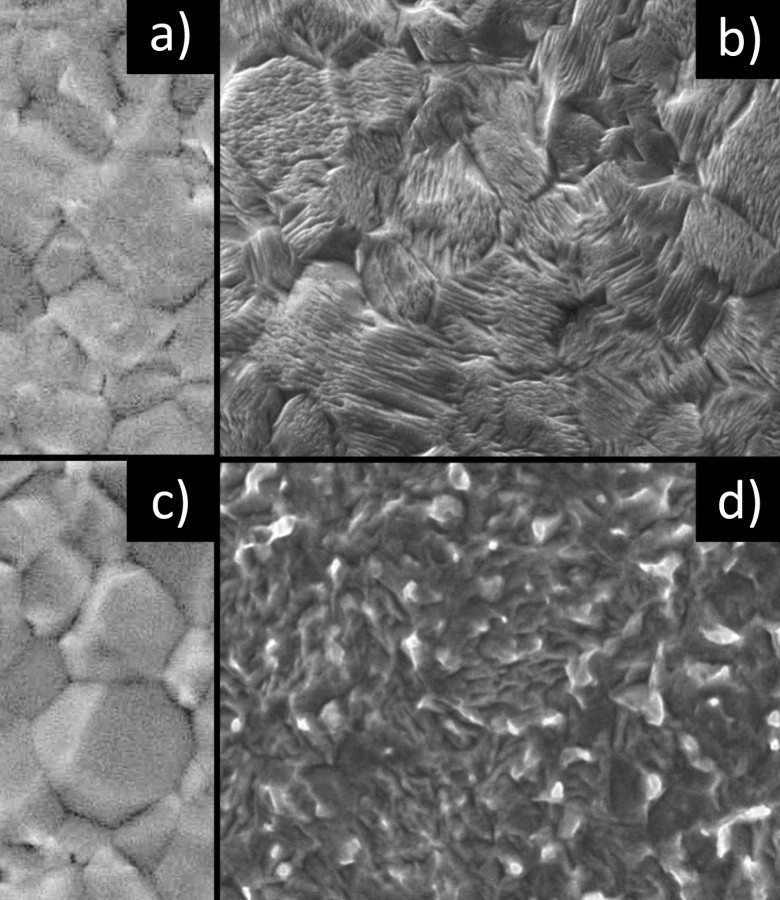 Fig. 8: SEM images (5000x magnification) of a) freshly deposited, unetched b) freshly deposited, etched c) aged, unetched and d) aged, etched (221)(321)-oriented tin layer Looking at the layer architecture of the freshly deposited and aged samples, it quickly becomes clear, as already mentioned several times, that grain boundary diffusion is decisive for or against whisker growth. This finding is in excellent agreement with the hypothesis derived from the 'Critical Angle Theory' that GBsa layers tend to exhibit significantly stronger whisker growth than GBla layers. Or to put it another way, the wider the grain boundary, the faster and the narrower the grain boundary, the slower the diffusion in the vertical direction and correspondingly more pronounced the risk of whisker formation, which is massively increased by cross-grain coalescence and grain boundary annihilation.
Ageing of large-angle grain boundary layers
But how do GBla tin layers age? As mentioned above, electrodeposited coatings tend to form GBsa textures. However, there are chemicals that are capable of counteracting the inherent tendency of electroplated layers to form GBsa textures and instead form GBla layers. Using such a process, whose tin layers are characterized by a mixed (101)(220)(211)(112) texture, the coatings and etching tests described above were repeated. Compared to the small-angle grain boundary layers, the large-angle grain boundary layers now deposited show a more angular appearance on the surface (Fig. 9a). However, the difference is particularly apparent after 10 seconds of etching (Fig. 9b), where much deeper trenches marking the grain boundaries are now observed than was the case in the first experiments. The difference between the GBsa layers and the aged samples is even more drastic (Fig. 9c). In contrast to the former, coalescence across grains no longer takes place. The grain boundaries remain open, which ensures continuous and, in particular, ubiquitous pressure reduction. Strictly speaking, these processes are not recrystallizations, but crystal recoveries, which by definition differ from the former precisely in that only small-angle and not large-angle grain boundaries are displaced [35].
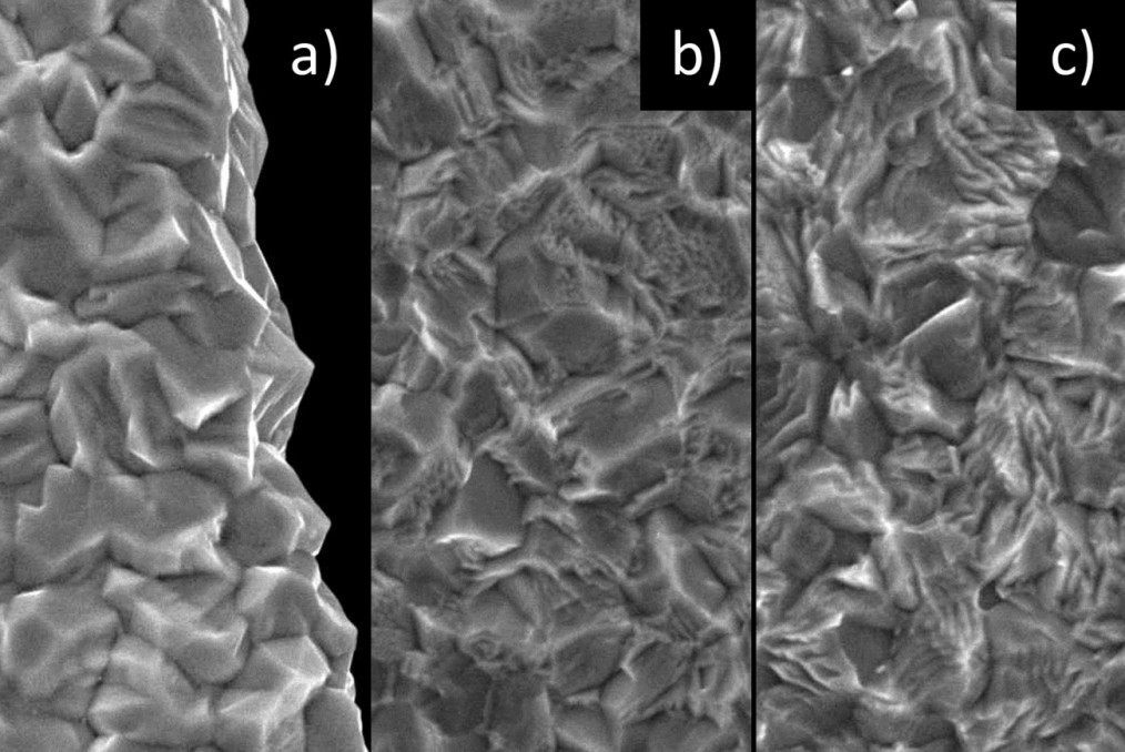 Fig. 9: SEM images (5000x magnification) of a) unetched b) freshly deposited, etched and c) aged, etched (101)(220)(211)(112)-oriented tin layer Perhaps the most impressive difference between GBsa and GBla layers can be seen when the corresponding aged layers are etched for five seconds (Fig. 10). While the GBsa layer is etched away relatively homogeneously (Fig. 10a), the etching attack on the GBla layer takes place much more strongly along the grain boundaries, leaving a landscape criss-crossed by trenches in which the individual grains almost appear to be detached (Fig. 10b). If we now look at GBsa layers from which whiskers are already growing (Fig. 10a), we find exactly the same type of trenches, but only around the growing whisker, whereas no whiskers could be observed in the GBla layer, which is interspersed with trenches. While the 'critical angle theory' on its own leaves much room for speculation, the etching experiments provide very direct evidence of the dramatic influence of the dimensions of the grain boundaries. However, the question of the influence of the substrate on whisker growth still remains unanswered.
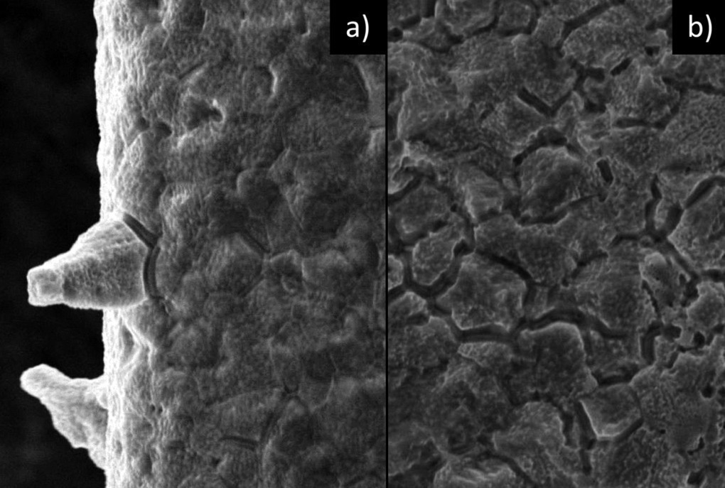 Fig. 10: SEM images (5000x magnification) of superficially (2 seconds) etched tin layers; a) (221)(321) texture, b) (101)(220)(211)(112) texture)
IMC wedge formation keeps diffusion channels open
For this purpose, the coating experiments described above on copper single crystals with (100) and (110) preferred orientation were extended accordingly by depositing GBla layers in addition to GBsa tin layers. In order to promote whisker growth, the ageing interval was extended to 21 days <br and since the focus was on the influence of the Cu6Sn5 crystals, the tin layers were completely etched off (Fig. 11). X-ray diffraction (ϑ-2ϑ scan) was used to verify that the applied tin layers actually had the corresponding textures, with the GBsa layers characterized by a (211)(321)(431) texture and the GBla layers by a (101)(220)(211)(112) texture.
The results fully met the expectations based on the preliminary tests: Very many whiskers in the combination of Cu(100) with GBsa(Fig. 11a), fewer whiskers in Cu(100) with GBla(Fig. 11b), significantly fewer whiskers in Cu(110) with GBsa(Fig. 11c) and no whiskers in Cu(110) with GBla layers (Fig. 11d). Also expected, but diametrically opposed to generally accepted theories, was that the number of whiskers decreased rapidly with increasing amounts of Cu6Sn5. The AFM images, which can also be used to determine the extent of IMC growth in the z-direction, show that not only the amount of IMC has increased, but also the grains that protrude deep into the tin structure. In fact, IMC crystals with a penetration depth of no less than 3.3 µm are found on (110) substrates, while the maximum value for (100) substrates is only 2.1 µm. This suggests that the IMC grains grown from and on (110) copper substrates actually perforate the tin layer. This means that the faster the intermetallic phase growth takes place, the sooner the grain boundaries and thus the vertical diffusion channels remain open.
![Abb. 11: AFM-Bilder (Contact-Modus, Kantenlänge 50 µm) nach vollständigem Abätzen der Schicht nach 21 Tagen Auslagerung bei Raumtemperatur; a) GBsa-Schicht auf Cu(100)-Einkristall, b) GBlaSchicht auf Cu(110)-Einkristall, c) GBsa-Schicht auf Cu(110)-Einkristall, d) GBla-Schicht auf Cu(110)-Einkristall (aus [6]) gt 2023 09 060](/images/stories/Abo-2023-09/gt-2023-09-060.jpg) Fig. 11: AFM images (contact mode, edge length 50 µm) after complete etching of the layer after 21 days of aging at room temperature; a) GBsa layer on Cu(100) single crystal, b) GBla layer on Cu(110) single crystal, c) GBsa layer on Cu(110) single crystal, d) GBla layer on Cu(110) single crystal (from [6]) In summary, two processes can be observed that have a decisive influence on the course for or against whisker growth. Firstly, the formation of intermetallic phase, which on the one hand is responsible for the pressure build-up in the layer and on the other hand causes exactly the opposite, namely pressure reduction by keeping the diffusion channels open along the grain boundaries. Secondly, the tin self-diffusion as part of a maturation process of the tin layer, which causes the grain boundaries to disappear across grains through coalescence and thus brings vertical diffusion to a standstill. Looking at the two extreme cases, strong whisker growth with the combination of GBsa tin on Cu(100) and no whisker growth with GBla tin on Cu(110), it becomes obvious that the ratio of the speeds of the two processes defines whether whiskers grow or not. With fast inter-grain coalescence and slow IMC formation, whiskers will grow; with fast IMC formation and slow coalescence, there is sufficient time for Cu6Sn5 wedges to form along the grain boundaries, preventing inter-grain coalescence and thus whisker growth.
Fig. 11: AFM images (contact mode, edge length 50 µm) after complete etching of the layer after 21 days of aging at room temperature; a) GBsa layer on Cu(100) single crystal, b) GBla layer on Cu(110) single crystal, c) GBsa layer on Cu(110) single crystal, d) GBla layer on Cu(110) single crystal (from [6]) In summary, two processes can be observed that have a decisive influence on the course for or against whisker growth. Firstly, the formation of intermetallic phase, which on the one hand is responsible for the pressure build-up in the layer and on the other hand causes exactly the opposite, namely pressure reduction by keeping the diffusion channels open along the grain boundaries. Secondly, the tin self-diffusion as part of a maturation process of the tin layer, which causes the grain boundaries to disappear across grains through coalescence and thus brings vertical diffusion to a standstill. Looking at the two extreme cases, strong whisker growth with the combination of GBsa tin on Cu(100) and no whisker growth with GBla tin on Cu(110), it becomes obvious that the ratio of the speeds of the two processes defines whether whiskers grow or not. With fast inter-grain coalescence and slow IMC formation, whiskers will grow; with fast IMC formation and slow coalescence, there is sufficient time for Cu6Sn5 wedges to form along the grain boundaries, preventing inter-grain coalescence and thus whisker growth.
To be continued in Galvanotechnik 10/2023
Literature
[1]WEEE Directive 2002/96/EC
[2]RoHS Directive 2002/95/EC
[3]ELV Directive 2000/53/EC
[4]Egli, A.; Zhang, W.; Heber, J.; Schwager, F.; Toben, M.: Where crystal planes meet: contribution to the understanding of the whisker growth process, IPC Annual Meeting S08/3/1-S08/3/5 (2002)
[5]Egli, A.; Zhang, W.; Schwager, F.: New approach to whisker free deposits, Proc. 5th EPTC 55-58 (2003)
[6] Zhang, W.; Egli, A.; Schwager, F.; Brown, N.: Investigation of Sn-Cu intermetallic compounds by AFM: new aspects of the role of intermetallic compounds in whisker formation, IEEE Trans. Electron. Packag. Manuf., 28, (2005) 85-93
[7] Egli, A.: iNEMI Report - Tin Deposit Ripening and Whisker Growth, ECTC Conference, Orlando (2005)
[8] Zhang, W.; Clauss, M.; Schwager, F.: Growth Behavior of Meta-Stable NiSn3 Intermetallic Compound and Its Potential Influence on the Reliability of Electronic Components, IEEE Trans. Compon. Pack. Manuf. Tech. 1, (2011) 1259-1268
[9] Cobb, H.L.: Cadmium Whiskers, Monthly Rev. Am. Electroplaters Soc. 33, (1946) 28-30
[10] Compton, K.G.; Mendizza, A.; Arnold, S.M.: Filamentary growth on metal surfaces - whiskers, Corrosion 7, (1951) 327-334
[11] Fisher, R.M.; Darken, L.S.; Carroll, K.G.: Accelerated growth of tin whiskers, Acta Metall. 2, (1954) 368-372
[12] Website of the NSF Center for Advanced Vehicle and Extreme Environment Electronics, retrieved October 20, 2022, Mechanism of Tin Whisker Growth in Electronics (auburn.edu)
[13] Website of the NASA Goddard Space Flight Center, retrieved October 20, 2022, Basic Info on Tin Whiskers. October 2022, Basic Info on Tin Whiskers (nasa.gov)
[14] Jagtap, P.; Jain, N.; Chason, E.: Whisker growth under a controlled driving force: Pressure induced whisker nucleation and growth, Scripta Mater. 182, (2020)43-47
[15] Pei, F.; Briant, C.L.; Kesari, H.; Bower, H.F.; Chason, E.: Scripta Mater. 93, (2014) 16-19
[16] Osenbach, J.W.; DeLucca, J.M.; Potteiger, B.D.; Amin, A.; Shook, R.L.; Baiocchi, F.A.: Sn Corrosion and Its Influence on Whisker Growth, IEEE Trans. Electron. Packag. Manuf. 30, (2007) 23-35
[17] Tu, K.N.: Interdiffusion and reaction in bimetallic Cu-Sn thin films, Acta Metall. 21, (1973) 347-354
[18] Tu, K.N.; Thompson, R.D.: Kinetics of interfacial reaction in bimetallic Cu-Sn thin films, Acta Metall. 30, (1982) 947-952
[19] Dunn, D.S.; Marinis, T.F.; Sherry, W.M.; Williams, C.J.: Dependence of Cu/Sn and Cu/60Sn40Pb solder joint strength on diffusion controlled growth of Cu3Sn and Cu6Sn5, Mat. Res. Soc. Symp. Proc. 40, (1985) 129-138
[20] Tu, K.N.: Irreversible processes of spontaneous whisker growth in bimetallic Cu-Sn thin-film reactions, Phys. Rev. B 49, (1994) 2030-2034
[21] Tu, K.N.; Li, J.C.M.: Spontaneous whisker growth on lead-free solder finishes, Mater. Sci. Engin. A 409, (2005) 131-139
[22] Hasiguti, R.R.: A tentative explanation of the accelerated growth of tin whiskers, Acta Metall. 3, (1955) 200-201
[23] Franks, J.: Metal whiskers, Nature 177, (1956) 984
[24] Franks, J.: Growth of whiskers in the solid state, Acta Metall. 6, (1958) 103-109
[25] Kehrer, H.-P.; Kadereit, H.G.: Tracer experiments on the growth of tin whiskers, Appl. Phys. Lett. 16, (1970) 411-412
[26] Boettinger, W.J.; Johnson, C.E.; Bendersky, L.A.; Moon, K.-W.; Stafford, G.R.: Whisker and Hillock formation on Sn, Sn-Cu and Sn-Pb electrodeposits, Acta Mater. 53, (2005) 5033-5050
[27] Arnold, S.M.: Repressing the Growth of Tin Whiskers, Plating 53, (1966) 96-99
[28] Britton, S.C.: Spontaneous Growth of Whiskers on Tin Coatings: 20 Years of Observation, Trans. IMF 52, (1974) 95-102
[29] Dunn, B.D.: A laboratory study of tin whisker growth, ESA Report STR-223, (1987) 1-51
[30] Mishin, Y.; Herzig, C.; Bernardini, J.; Gust, W.: Grain boundary diffusion: fundamentals to recent developments, Intern. Mater. Rev. 42, (1997) 155-178
[31] Zhang, W.; Egli, A.: Unpublished results
[32] Egli, A.: Tin Plating Method, EP 1 342 816 (2003)
[33] Kuhr, T.A.; Sanchez, E.K.; Skowronski, M.; Vetter, W.M.; Dudley, M.: Hexagonal voids and the formation of micropipes during SiC sublimation growth, J. Appl. Phys. 89, (2001) 4625-4630
[34] Zhang, W.; Egli, A.: Unpublished results
[35] Doherty, R.D.; Hughes, D.A.; Humphreys, F.J.; Jonas, J.J.; Juul Jensen, D.; Kassner, M.E. et al.: Current issues in recrystallization: a review, Mater. Sci. Engin. A 238, (1997) 219-274


