
If you browse through a British encyclopaedia, you get the impression that everything was invented by the British. This opinion changes when you pick up an American one, in which Americans are the inventors. In French ones they are French, in German ones German and in Russian ones only Russian.
 Fig. 2: Eisler's radio with circuit boardWhetherBerthold Schwarz invented the powder in Freiburg i. Br. or the Chinese a few hundred years earlier is just as absurd a discussion as the one about Meissen porcelain. Why is it so important what nationality the inventor was, when the Neanderthals (or Homo heidelbergensis), who obviously used the spear and could therefore be considered inventors, lived on what is now German soil, but hardly considered themselves German?
Such peculiar claims are also made in the electronics industry. On the one hand, it is said to have been the American Charles Ducas (US patent US1563731A) who came up with the basic idea for the printed circuit board in 1925. This is contradicted by those who cling to the German Albert Hanson, who patented a flat foil conductor on an insulating board with several layers in England as early as 1903, which may not have looked like a modern printed circuit board, but still had many of the basic properties.
Again in England, there is a patent from the Austrian inventor Paul Eisler that came closer to the mark. Eisler's 1943 patent application was eventually split into three separate patents: 639111 (three-dimensional printed circuits), 639178 (foil technology of printed circuits) and 639179 (powder printing) and published in 1950. He himself built a radio using these ideas, but it should come as no surprise that the first printed circuit boards were then used in weapon systems.
Many people had the idea of regulating the wire in electronic products and laboratories. Thomas Edison, for example, experimented with chemical methods for coating conductors on linen paper as early as 1904. Arthur Berry's 1913 patent in the UK describing a printing and etching process is also relevant, and in the USA Max Schoop was granted a patent for spraying metal through a mask as a pattern on a plate. As is so often the case, the breakthrough came about because people were not satisfied with the current state of affairs.
Certainly one of the reasons was that a tangle of wires could only be soldered by hand and therefore mass production was only possible with many workers, which led to increased risk in the products due to the unreliability of manual work.
 Fig. 3: Wave soldering according to Barnes and Strauss - should solder 'flawlessly'!
") Fig. 4: Television set from 1948 still without LP (Motorola)With the printed circuit board, all potential soldering points were suddenly offered on one level, which was a tempting sign of automation. In fact, on October 3, 1956, Allan Barnes, Vic Elliot and Ralph Strauss (all of Fry's Metals) applied for a patent for a new invention, which was granted on July 23, 1958. Allan Barnes, a scientist, and Ralph Strauss, a flux chemist, had invented wave soldering, which then helped advance electronic manufacturing for years.
Fig. 4: Television set from 1948 still without LP (Motorola)With the printed circuit board, all potential soldering points were suddenly offered on one level, which was a tempting sign of automation. In fact, on October 3, 1956, Allan Barnes, Vic Elliot and Ralph Strauss (all of Fry's Metals) applied for a patent for a new invention, which was granted on July 23, 1958. Allan Barnes, a scientist, and Ralph Strauss, a flux chemist, had invented wave soldering, which then helped advance electronic manufacturing for years.
From the various efforts, you can see that they experimented with all kinds of base materials. Almost everything from Bakelite and Masonite to thin sheets of wood were used as early PCB materials. Holes were drilled, brass wires were riveted to them and components were placed on and in them. Old radios and gramophones still occasionally contain such products.
In the meantime, the Americans were torn from their contemplative rest when they heard Russian beeps from space:
- Launch of the first satellite, Sputnik, in 1957
- Launch of the first spacecraft, Luna 2, to the moon in 1959
- Sending the first cosmonaut, Yuri Gagarin, around the Earth in 1961
Although double-sided printed circuit boards with through-hole plating were already available in 1947, it was not until 1963 that the Hazeltyne Corporation [1] applied for a patent for the first through-hole plating. Now it was possible to place components much closer together. As the wave soldering process was already available, mass production really took off. The increased budgets of institutions such as NASA also helped. The US space budget increased fivefold in 1960!
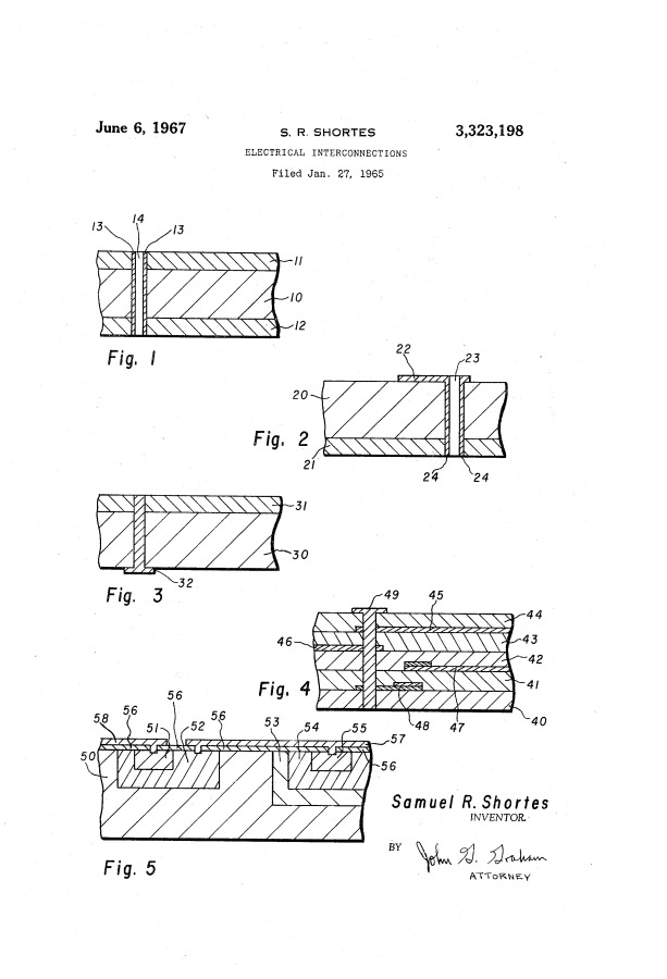 As can be seen from the illustration of patent 3323198, multilayer printed circuit boards were already known. Printed circuit boards with four or more layers had already gone into production in 1960. What was still missing were processes that simplified production. Design was also still lagging behind, as almost everything still had to be designed by hand. Special programs had to be developed, which were soon introduced.
The first transistor still looks a bit large and strange, but soon it was possible to fit several on a silicon plate and nowadays it is possible to do considerably more. At present, TSMC and Samsung in South Korea are the only manufacturers in the world that can produce first-class 7-nanometer chips with more than 10 billion transistors.
The second breakthrough that changed everything was the invention of the integrated circuit [2], which soon led to the mainframe computer. Computers and everything to do with them have become an integral part of the world. From the first hand-held telephone or the first electronic calculator to today's laptop or mobile phone, it is a path that has been traversed in a very short time.
No self-respecting seven-year-old is surprised that her smartphone not only connects her with her friends, but also stores all their phone numbers and addresses. She can also call up her favorite games and listen to music. The device also functions as an alarm clock and watch and, if necessary, as a flashlight. She photographs and films her cat and uploads it all to the Internet. And she has by no means exhausted all the capabilities that her father might use.
The pressure on the circuit board has led to new production methods, ranging from EDA (Protel [3] & EAGLE [4]) to fully automated production. In between, surface mounting, which was developed in Japan on the model of hybrid circuits, came buried components in the intermediate layers, which made everything shrink, and finally the three-dimensional specifications.
") Fig. 6: First transistor in 1947 (Bell Labs )
Fig. 6: First transistor in 1947 (Bell Labs )
 Fig. 7: Inverted F-antenna, printed with CB028 on 3D-printed, brominated ABS phone case - before attaching the base plate
") Fig. 8: 3D structural electronics (Keck Center, University of Texas at El Paso)
Fig. 8: 3D structural electronics (Keck Center, University of Texas at El Paso)
After IBM once used the inside of a typewriter casing as a printed circuit board, in future there will be an increasing move towards completely new manufacturing methods, such as printing the three-dimensional printed circuit board together with the associated cables and components.
On the other hand, we must not lose sight of the photon because of the amount of data. As more and more data is used and utilized, the electrical metal conductor will be increasingly supplemented by optical conductors and perhaps the printed circuit board of the future will be a glass pane?
Literature:
K. Church et al: Turning Printed Circuit Boards Into Printed Circuit Structures Using 3D Printing, army contract # W911NF13-1-0109, US ARMY RDECOM ACQ CTR - W911NF, Title: HBCU/MI: 3D Formable RF Mat
D. Geiger; G. Thein: 3D Assembly Processes a Look at Today and Tomorrow, IPC APEX EXPO Conference Proceedings
J. Schwietering: The Glassy Future of Circuit Boards, 30.04.2020; Fraunhofer/IZM
References
[1] en.wikipedia.org/wiki/Hazeltine_Corporation
[2] 1958 by Jack Kilby at Texas Instruments
[3] en.wikipedia.org/wiki/Altium_Designer
[4] en.wikipedia.org/wiki/EAGLE_(program)
About the person
Prof. Rahn is a globally active consultant in connection technology. His new book on 'Special Reflow Processes' was recently published by Leuze Verlag. He can be contacted at
