
Spatial circuit carriers (3D-MID), which have been continuously developed since entering the market around 25 years ago, are increasingly present on the market. The reasons for this are miniaturization and weight reduction. The possibilities of incorporating mechanical, sensory, optical, fluidic and thermal functionalities into 3D modules are far from exhausted.
In the introduction to Part 1, which had Printed Electronics (PE) as its core topic, the author already went into some basic things about 3D-MID. For many, the letter M in the abbreviation stands for 'Mechatronic' instead of 'Molded'. In fact, according to [1], the original term Molded Interconnect Devices was already renamed Mechatronic Integrated Devices during the MID Congress 2010. Nevertheless, the term molded persists, which is not wrong in itself from the perspective of the history of the development of 3D-MID. It reflected the integration of mechanical and electrical functions in injection-molded three-dimensional basic bodies, but does not do justice to today's broader understanding of 3D-MID. In its original form, it is about injection-moulded parts made of thermoplastic materials on which structured conductor patterns are realized and passive and active components are mounted using various techniques(Fig. 1).
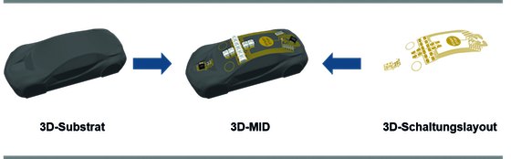 Fig. 1: Basic principle of 3D-MID [1]
If one assumes MID as mechatronic integrated devices, this includes the trend that these molded parts can also be manufactured from materials other than thermoplastics and using processes other than injection molding. At the same time, it is better expressed that mechanical and electrical, but also other functionalities such as sensory, optical, fluidic and thermal functions can be incorporated. The list of manufacturing processes for 3D-MID in [1] alone gives an impression of how differentiated these have become in recent years:
- 3D mask
- Laser resist or laser direct
- Flamecon
- Laser direct structuring (LDS)
- Primer - pad printing
- Mold stamp
- 2K injection molding
- Aerosol jet
- Conv. flex film
- Plasmadust
Nevertheless, the core steps of the most common production methods for the conductor pattern on 3D-MID are partly based on process steps that are also used in classic PCB production. These include chemical copper, electrolytic copper and etching processes. However, automated thermokinetic application processes such as Flamecon rely on high temperatures.
In the aerosol jet process, all solutions, pastes and suspensions can be used as coating materials (conductor, semiconductor, resistor and insulating materials) whose viscosity can be adapted to the system requirements by diluting them with a suitable solvent. However, the particle size of the solid material must be in the nanoscale range. This means that there are certain similarities with printed electronics in the realization of the electrical circuit. However, conventional thermal sintering processes are often used to harden the layers.
Some people therefore put printed electronics in the same 'drawer' as 3D-MID, but this is not correct in principle. The author is somewhat more familiar with 3D-MID than with PE, because he had to deal with it at a very early stage.
In both product directions, it is difficult to determine how many companies worldwide are actually involved in their production. Based on overviews of European and Japanese 3D-MID associations, the author estimated that around 50 companies worldwide manufacture 3D-MID products. These are flanked by a much larger number of suppliers who act as material, equipment and design service providers.
3D-MID market
When it comes to estimating the size of the 3D-MID market, the same uncertainties persist as with PE. Despite numerous inquiries at international electronics trade fairs such as JPCA or electronica, the author did not receive any satisfactory definitive answers regarding the annual production volume. For example, it was assumed that the value of 3D-MID was somewhere between 500 million and 1 billion dollars. In contrast to the many offers of market analyses on printed electronics, there is little analytical material on 3D-MID. A search for such material on the Internet (search term 3D MID Trend Analysis or Market Report, for example) produces almost only hits on 3D printing or 3D printers. However, this proves that this completely different and incomparable technology has now penetrated much more into industrial and private use than 3D MID. The technological and material diversity of 3D printing also appears to be much greater than that of 3D MID.
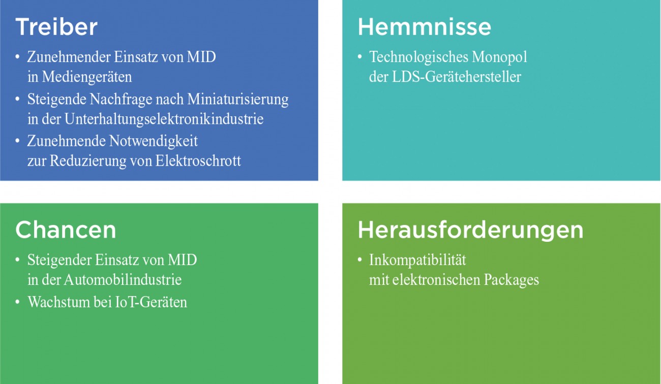 Fig. 2: Drivers, challenges and obstacles in the market development of 3D-MID products [2]
Some market analysts dare to offer predictions down to one decimal place. For example, in a commentary in the Daily News back in 2016, the author argued that a trend report at the time stated that the market size for 3D-MID is expected to increase to $629.5 million by 2023 with a compound annual growth rate (CAGR) of 13.8%. A forecast accurate to within $0.5 million at this high figure - that's very impressive! If this forecast comes true with an accuracy of 1 %, the author undertook at the time to roll a peanut from New York to San Francisco with his nose - which would be just as difficult to fulfill.
 Fig. 3: 3D-MID antenna for a smartphone from Laser Micronic based on LPKF's LDS technology
One of the few market research companies dealing with 3D-MID is the Indian company Markets-andMarkets Research Private Ltd. which also has a subsidiary in the USA in Northbrook (Illinois). It, too, follows the motto described above of providing overly precise trend figures. One example: In its report Molded Interconnect Device (MID) Market, which looks at the period 2017-2023, it states the following [2]:
The global MID market was estimated at $684.2 million in 2017 and was expected to reach $894.1 million in 2018. By 2023, it is estimated to increase to $1798.3 million at a CAGR of 15.0% during the forecast period. The base year for the surveys is 2017 and the forecast period is 2018-2023, meaning that revenue is expected to roughly double within six years. You don't know whether to laugh or be annoyed at the accuracy of the figures.
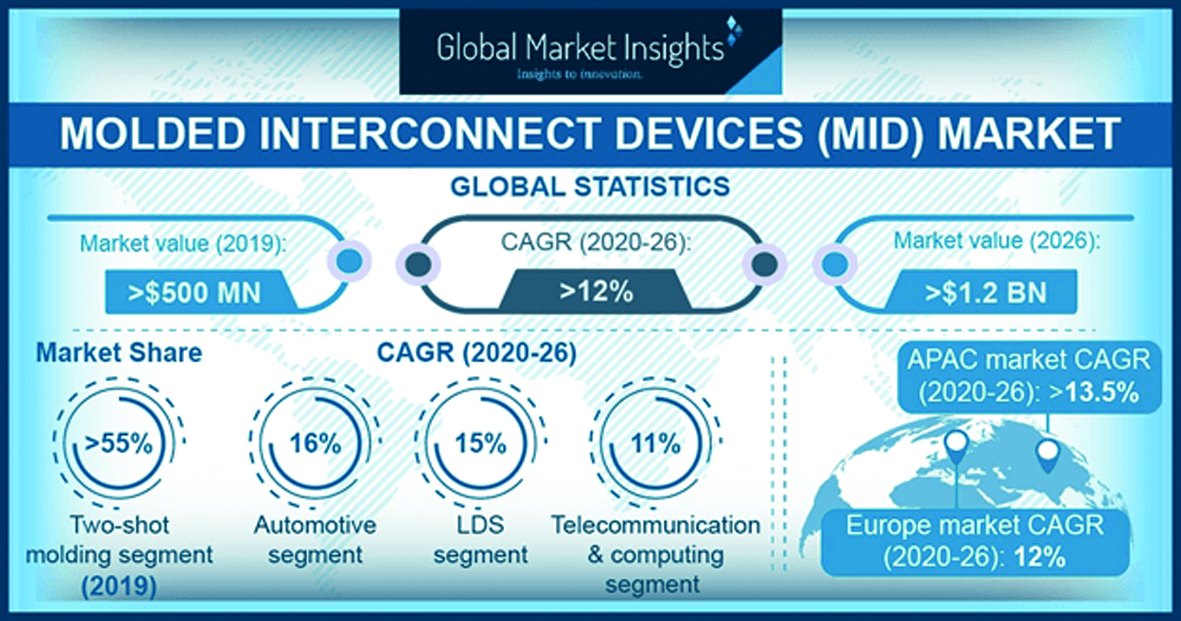 Fig. 4: Examples of statements in the market analysis by Global Market Insights for the years 2020-2026 One reason given for the rapid forward development of the 3D-MID market at the time was that portable electronic devices that have multiple functions in miniaturized small housings or modules are gaining in importance, for example in consumer and medical electronics. In order to meet the requirements of miniaturization, it is expedient to combine mechanical and electrical systems in a complete product. This can be achieved with the help of MIDs.
In a graphic, the company gives examples of driving forces, challenges and obstacles(Fig. 2). Not only the Indian market analysis company Markets-andMarkets provides over-accurate market figures, but also the US-Indian company Transparency Market Research. It is difficult to determine whether it is essentially an American or Indian company, as it has two offices: in Albany (USA) and in Pune (India) [3]. The term 'headquarters' does not appear. However, the way the figures are presented speaks more in favor of an Indian company. In August 2018, Transparency Market Research published the study '3D Printed Electronics Market - Global Industry Analysis, Size, Share, Growth, Trends, and Forecast, 2018-2026'. It treats 3D-MID as a subgroup of 3D printed electronics. The results of this study are difficult to utilize.
The US market analysis company Global Market Insights Inc (Selbyville, Delaware) comes up with completely different, more modest figures. Its 3D-MID market forecast has the base year 2019 as and makes the following predictions for the period 2020-2026 [4]:
The 3D-MID market exceeded $500 million in 2019. It will reach a value of USD 1.2 billion or more in 2026 with a CAGR of over 12% between 2020 and 2026. As with MarketsandMarkets, sales are expected to at least double within six years, albeit a few years later than in India and at significantly lower values. However, both forecasts indicate a very high development and penetration dynamic for 3D-MID.
According to the Americans, the strong market growth is due to the increasing acceptance of the electromechanical functions of 3D-MID in electronics solutions for very different industries, because they
- reduces assembly times and production costs
- increases circuit density and reduces weight
- simplifies the introduction of 3D-MID in military technology
- results in a high degree of design freedom.
As always, these significant differences in the figures in the forecasts of the respective market research companies are due, among other things, to the fact that
- the data basis available for the analyses is different
- the definition of the technologies, components and application sectors to be considered is different
- the geographical regions included differ.
Global Market Insights writes that MIDs have a high reliability and a low failure rate, which means that fewer auxiliary components are required and this in turn leads to a relative reduction in the complexity of the systems. This means, among other things, that fewer discrete additional components are required to implement a specific function in a module/device/system.
These properties contribute to the increasing demand in the automotive, military, consumer electronics and telecommunications sectors, for example. In cell phones in particular, 3D MID components can reduce volume and make more efficient use of space, for example through an internal MID antenna. Figure 3 shows an example of the creation of a 3D MID antenna for a smartphone from Laser Micronic, manufactured using LPKF's LDS technology.
In addition, 3D MID technology offers the advantage of increasing the aesthetic value of cell phones through its flexible properties. For example, the coating and shaping properties of MIDs can be used to modify the product variation and offer different colors and shapes. Cell phones, laptops and tablets are expected to play a significant role in the advancement of 3D MID technology in the coming years.
Figure 4 contains some extracted data from the study, e.g. that two-shot molding (also known as 2k mold or double injection molding) predominated among manufacturers in 2019 with a 55% share and that laser direct structuring (LDS) still has room for expansion with a 15% share. There are a large number of variants of two-component injection molding, which cannot be discussed in detail here for reasons of space. Interested parties can find more information at [1]. Figure 5 clearly reflects the different penetration rates of 3D-MID technology in individual application areas in the forecast period.
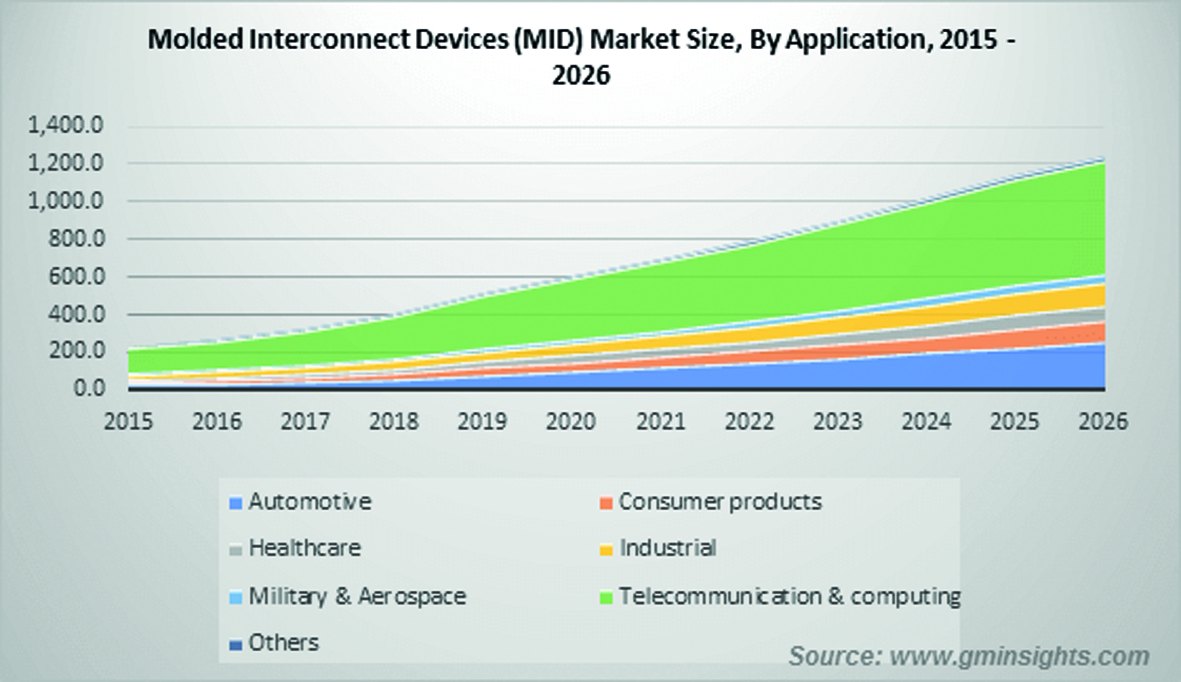 Fig. 5: Different penetration rates of 3D-MID components in the various application areas 2015-2026
Automotive applications held a market share of 16% in 2019 and will record growth of around 16% by 2026. This is due to the increasing use of 3D-MID components in a variety of automotive applications, including brake sensors, steering wheel hubs, lighting and position sensors. However, applications in telecommunications and computer technology will show the greatest growth, as already mentioned above for smartphones.
The market analysis by Global Market Insights demonstrates how diverse the drivers for the advance of 3D-MID technology are:
- Rapid spread of wearables in the USA
- Favorable regulatory scenario for the reduction of electronic waste in the European Union
- High demand from the automotive industry in Germany, France and Italy
- Rising demand for smartphones in the Asia-Pacific region
- Growth of the semiconductor manufacturing industry in China, South Korea, Taiwan.
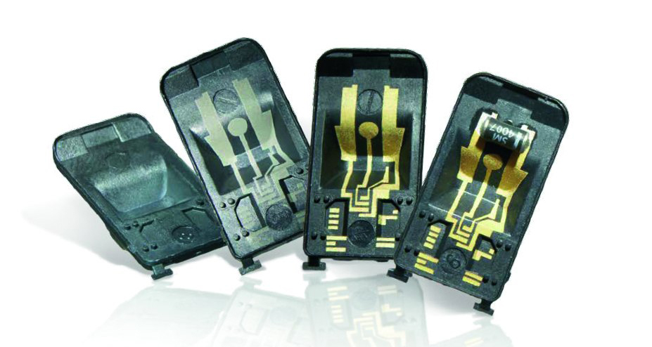 Fig. 6: Basic steps of the LPKF LDS process. Image: LPKFHowever, if you compare the figures provided by Markets-andMarkets and Global Market Insights for the development of the 3D-MID market up to 2023 (MarketsandMarkets) and 2026 (Global Market Insights) with the revenue figures expected for printed electronics according to Part 1 of this article, there is a world of difference. In 2026, printed electronics will already have a production value significantly several times that of 3D-MID, while classic printed circuit boards (rigid, flexible and rigid-flexible) will be many times higher. If we compare 3D-MID products with printed electronics and traditional PCBs, the former will remain a relative niche product for a long time to come. This is also supported by the fact that some printed electronics products could well become competitors to 3D-MID products in the future and overtake them. One of the reasons for this could be the non-environmentally friendly chemical and highly thermal processes used in today's PCB production, some of which are also used in 3D-MID production.
Personal experience with 3D-MID
At the beginning of the 1980s, the author was involved in MID development at the US company PCK Technology, where he was employed at the time. A 2-shot molding process was used for a simple circuit. However, as the complexity of the circuits grew, their design increasingly proved to be a nightmare. However, once they were designed and the two parts successfully molded, the subsequent copper plating proved to be a breeze. All you had to do was place the parts to be plated in a basket and immerse them in an electroless copper plating bath. Today, the majority of MIDs are produced by laser direct imaging (LDS). In the author's opinion, this will also be the main trend in the future. He also considers the market share of S-short molding to be realistic at around 80 %.
At the time, Kodak took a license from PCK Technology and produced MID in a small subsidiary for several years. Their design was difficult and the price of 3D MID modules was much higher than normal PCBs for the same function. Three-dimensional assembly also proved to be problematic. There is no doubt that MIDs will have their place in the PCB market, but predicting the size in seven years is quite difficult from his point of view.
A couple of colleagues at the PCK Technology Division of Kollmorgen Corporation (a spin-off of the research and development division of Photocircuits Corporation), where the author worked from 1975 to 1990, developed the 2-shot method. PCK was the world champion of fully additive (chemical) electroplating, called CC-4, and 2-shot molding was based on this additive coating.
 Fig. 7: Use of laser direct structuring for conductor pattern generation (LDS) The first mold is produced with thermoplastic powders in which Pd is dispersed. The second molded part is then produced with a plastic without Pd, which covers the first part in which no conductor tracks are to be formed. The finished molded parts are then exposed to a permanent aganate solution in order to activate the first molded part, which then becomes receptive for the subsequent electroless copper plating.
This 2-shot molding was later abandoned because the cost of the tool was too high and it was not suitable for the complex tool design required. For all the good things said about the 3D-MID process, there is one problem, and that is the cost of the mold. Unless the number of 3D-MID modules required reaches hundreds of thousands, the mold cost makes 3D-MID uneconomical.
3D-MID on the basis of LDS
The German company LPKF Laser & Electronics AG came up with the idea of laser direct structuring (LDS) [5]. Today, LDS is the most important 3D-MID process. The company exhibits at every conceivable trade fair, including electronica, productronica and the JPCA show in Tokyo. Figure 6 shows the four basic steps of the LPKF LDS process, Figure 7 the laser structuring.
- Step 1: The laser-structurable molded parts are produced using single-component injection molding from commercially available plastic with additives.
- Step 2: The IR laser beam selectively structures the conductive pattern. The thermoplastic material is activated by the laser energy. A physical-chemical reaction creates metallic cores - this is the activation process. In addition to activation, the laser forms a microrough surface on which the copper is firmly anchored during metallization.
- Step 3: The metallization of LDS parts begins with a cleaning step. This is followed by an additive conductor build-up in electroless copper baths, typically in the order of 8 to 12 μm/h. This is usually followed by an electroless plating of nickel and a thin layer of gold. Application-specific coatings such as Sn, Ag, Pd/Au, OSP etc. can also be applied in this process. The finest conductor structures are less than 100 µm wide.
- Step 4: Many laser-activatable plastics with high heat resistance such as LCP, PA 6/6T or PBT/PET blend are reflow solderable and therefore compatible with standard SMT processes. Dispensing is the standard process for solder paste application when different height levels need to be achieved. There are a number of suppliers of technical solutions for three-dimensional placement.
LPKF LDS technology can be used to produce reliable vias to connect the surfaces of MIDs. This expands the possibilities of the layout. Figure 8 demonstrates the corner parameters of 3D-MID as achieved at Harting:
- Minimum value for distances between the conductor tracks (a): 50-150 μm
- Minimum width of the conductor tracks (b): 50-150 μm
- Radius (r): 0.2 mm
In contrast to classic PCBs, one of the major advantages of 3D-MID from an environmental perspective is that they are made from recyclable thermoplastics and are easier to dispose of.
The advantages now include the fact that large components can also be produced using the LDS process, for example with the LPKF Fusion3D 1500(Fig. 9). The working area of the machine is max. 2 x 400 mm x 78 mm x 80 mm (L x W x H). The scan field of the processing unit is 160 x 160 x 80 mm.
The initial costs for 3D-MID are considered to be relatively low. Equipped with the latest components and a high-quality rotary indexing table, the LPKF Fusion3D 1200 machine can be used to produce small, medium and large series of 3D circuit carriers particularly economically.
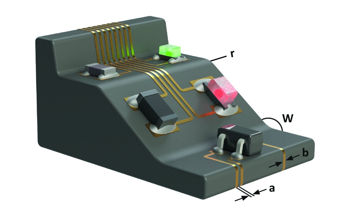 Fig. 8: Key parameters of 3D-MID at Harting
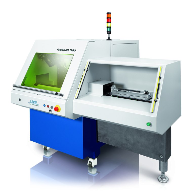 Fig. 9: LPKF Fusion3D 1500 for the production of large components using the LDS process
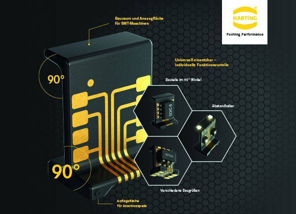 Fig. 10: Examples of different SMD components mounted on the 3D-MID component carriers from Harting
Suppliers and manufacturers
Most suppliers for 3D MID production as well as the manufacturers themselves are organized in corresponding interest groups in Germany and Japan, for example: www.3dmid.de and www.jmid.gr.jp respectively. The Japan MID Association was reformed as a new organization in March 2020. The German 3D MID Association launched its new website in March 2020 and published a new 20-page image brochure at www.unserebroschuere.de/3dmid in summer 2020.
It is based in Nuremberg and claims to have 99 members. They are a mixture of 3D MID producers, material and machine manufacturers, users and R&D facilities. Around a third appear to be involved in MID production. BMW, Denso, Fiat-Chrysler, Daimler, Continental etc. are members from the automotive industry. Five Fraunhofer Institutes are listed in the directory. The University of Erlangen (FAPS) plays a central role in R&D activities as a major source of 3D-MID technology.
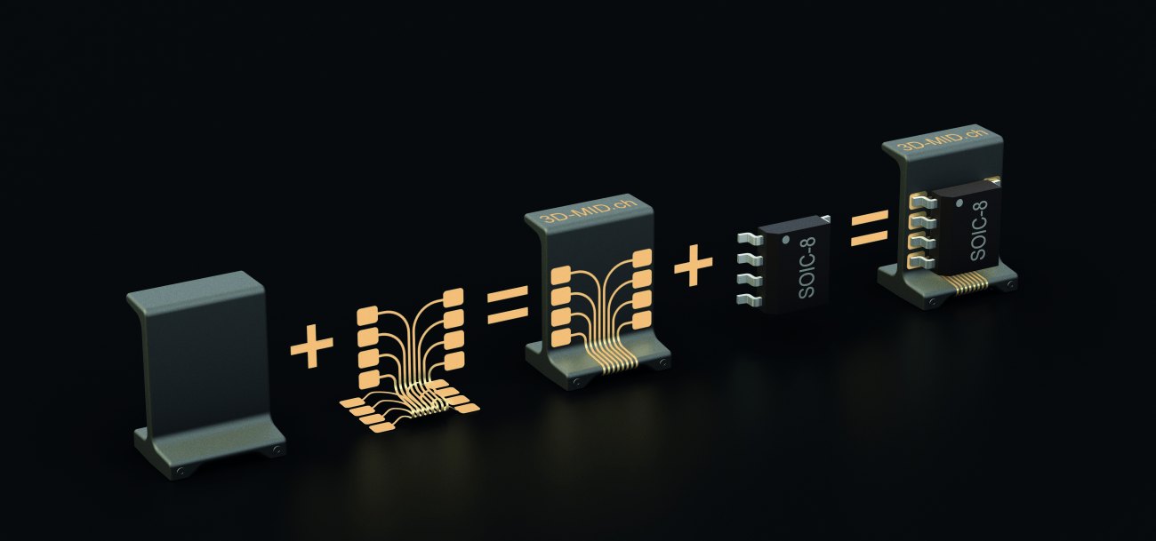 Fig. 11: Development of Harting's 3D-MID component carriers as a replacement for flexible circuits
One of the producers is Hahn-Schickard-Gesellschaft für angewandte Forschung e. V. In addition to research/development, its range of services also includes the production of small and medium-sized series as well as the transition to large-scale production [6]. The company has developed two process chains for the rapid prototyping of 3D-MID.
According to trade association overviews, other companies involved in 3D-MID are, for example: Zuken, Eagle, MID Solutions, Keeling & Walker, Ensinger Plastics, IBL, MacDermid Alpha, Mitsubishi Engineering Plastic, Teprosa, Sankyo Chemical, Panasonic, Johnan Corporation, Molex, MacDermid, Kato Precison.
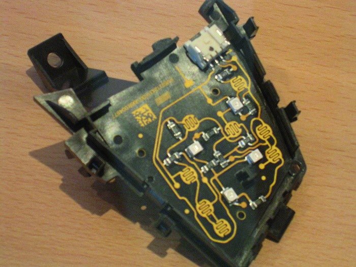
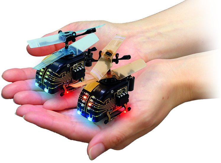 Fig. 12: Position sensor for adaptive speed control from Harting
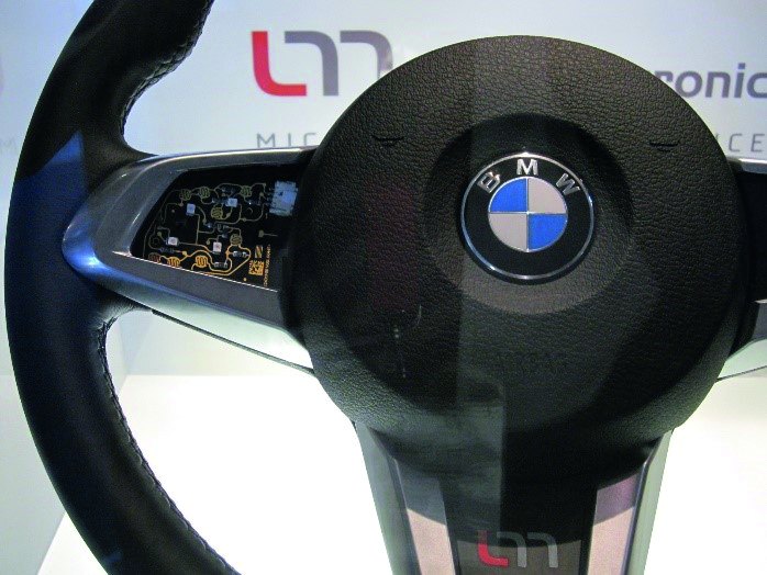 Fig. 13: Module for car control...
 ...at BMW
A few companies are highlighted below. Harting Mitronics is the largest producer of 3D-MID outside Asia and manufactures them at its plant in Biel/Switzerland. The only strange thing is that Harting allegedly only employs around 20 people for this purpose. You can watch several videos of the production process on YouTube. High-performance laser systems with three lasers working in parallel, each offset by 45 degrees, are used. Thanks to the additional axis of rotation, components can be processed by the laser simultaneously from all sides at 360 degrees. This enables flexible geometric shapes, such as reflector shells or LED lights. Despite the low conductor track thickness of 16 to 20 μm, the conductor tracks are suitable for demanding automotive components or for applications with currents of up to 10 A, such as heating coils for cameras that prevent fogging of the optics. Harting is said to be the only 3D MID manufacturer in the world to have a laser system with three 50 μm fine-focus optics.
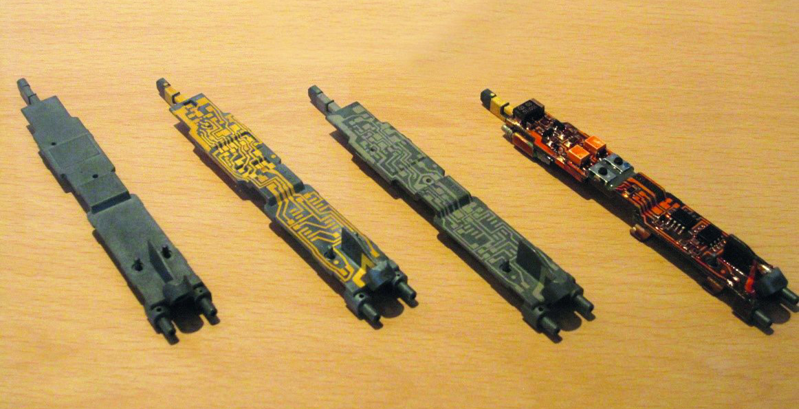 Fig. 14: Dental tool from Laser Micronics
As a medium-sized technology company in Magdeburg, Teprosa is active in the fields of 3D-MID, testing and inspection of electromechanical assemblies and laser fine machining. It sees itself as a full-service provider for 3D MID: injection moulding, LDS, metallization, assembly. Johnan Corporation (Kyoto, Japan) states that it uses 3D mounters from Yamaha and processes minimum chip dimensions of 0402 with them. The placement accuracy is a minimum of 40 µ and the pitch width is 80 µm. The same mounting values are specified for 2D SMT PCBs. Zuken provides the design tools for 3D-MID, while the Nuremberg-based company Neotech AMT GmbH provides a machine for economical rapid prototyping in the form of the PJ 15X.
The Japanese PCB manufacturers CMK and Kyoden appear to be interested in 3D-MID. However, they are very tight-lipped about providing more detailed information. Therefore, it is impossible even for this author to know the production scale of 3D-MID in Japan. Taiyo Ink is promoting photo-solder resists for 3D structures.
Product examples
Most manufacturers show the same samples every year at the JPCA show and also at electronica Munich. Cell phone antennas are the most advertised MID products. Some automotive and medical technology applications are also exhibited. However, as already mentioned, the injection mold is not cheap. Therefore, to justify the cost advantage, the number of pieces for each part must be much more than 100,000.
Figures 10 to 19 show samples taken by the author at various trade fairs or taken from the manufacturers' websites. However, they also include new products.
Harting, for example, presented a new 3D-MID solution in May 2020, in which standardized 3D-MID component carriers can take over the function of flexible printed circuit boards in some cases(Fig. 10 and 11). The components are mounted on these 3D-MID carriers instead of on flexcircuits as intermediate carriers and can be assembled fully automatically on PCBs in pick-and-place machines. The 3D-MID component carriers thus serve as a link between the component and the rigid PCB.

 Fig. 16: 3D-MID modules from Panasonic for the medical device and camera sector
Figures 12, 13 and 14 contain examples of exhibits from electronica. LPKF offers laser micromaterial processing services under the Laser Micronics brand.
The Magdeburg-based company Teprosa exhibited a small drone at the joint 3D-MID stand at productronica 2017, which clearly demonstrated the possibilities of this technology(Fig. 15). The Japanese companies Kyoden and Johnan also exhibited drones manufactured using 3D-MID technology(Fig. 17). These devices seem to be particularly popular for demonstrating the technical possibilities of 3D-MID technology. However, the many practical applications should not be forgotten, which can be demonstrated with exemplary 3D modules from Panasonic and Molex Japan for devices in the medical and camera sectors(Fig. 16, 18, 19). Molex Japan combined 3D MID technology with LDS antenna know-how to enable shielded, integrated fine pitch 3D circuits in a single module for medical devices and other high component density applications.
Fig. 17: Drone from Johnan
 Fig. 18: 3D MID module from Molex Japan for medical technology
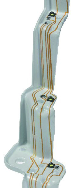 Fig. 19: Powder-coated 3D-MID module for automotive lamps from Molex
Translation, editing and additions: Dr. Hartmut Poschmann
References:
[2] www.marketsandmarkets.com/Market-Reports/molded-interconnect-device-market-150539319.html
[3] www.transparencymarketresearch.com/3d-printed-electronics-market.html
[4] www.gminsights.com/industry-analysis/molded-interconnect-devices-MID-market
[5] www.lpkf.com
[7] www.teprosa.de
[8] www.harting.com/3D-MID/en-gb/news/product/component-carrier-now-replacing-flexible-pcb
