The second of KSG's webinars on 3D PCBs took place at the end of January. Topic: 'Constructing, designing and optimally using multidimensional PCBs' PLUS 1/2021 reported on the first webinar (on rigid-flex, semi-flex and HSMtec assemblies).
In the second webinar, the various structures, functional principles and technologies of rigid-flex, semi-flex and HSMtec PCBs were presented. The decision as to which structures and PCB types are used in the assembly depends on the respective technical requirements that the PCB has to fulfill.
Choosing the right technology
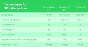
The production of printed circuit board assemblies varies in complexity and determines the costs, among other things. The choice of base material also influences the costs. For example, high-quality polyimide is used for rigid-flex structures in the bending area. Rigid-flex structures are also the most complex to manufacture, making them the most expensive compared to semiflex and HMSTec PCBs. In return, they meet high requirements, e.g. in terms of bending radius and cycles as well as impedance control.  The selection of the appropriate technology depends on the specific requirements of the PCB
General design rules
The sometimes highly complex technologies for rigid-flex, semi-flex and HSMtec PCBs require corresponding rules for the PCB design - the following design specifications apply:
- Conductor tracks must run in a straight line at right angles to the bending axis and ≥ 1 mm into the rigid area
- No holes in the area < 700 µm from the rigid-flex transition
- Fill copper-free areas in the bending area with copper
- Additional copper dummy conductors at the edges of the bending areas depending on the space (protection against scribing)
- Reduce the notch effect in the flex area with smooth transitions
- To improve flexibility, wide conductor tracks should be broken up into redundant individual conductors
- In the flex area, rasterize large copper areas if possible
- Avoid differences in wiring density in the flex area
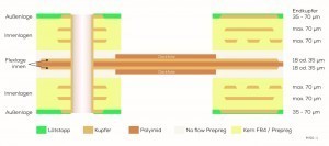
The different complex manufacturing processes for rigid-flex, semi-flex and HMSTec boards result in different and varied design recommendations - based on the following criteria, among others:  Eight copper profiles are integrated into the 4-layer HSMtec PCB for complete mechanical and electrical connection technology (below)
- Conductor width and conductor spacing
- End and pad diameter of the through-hole plating
- Length of the bending area
- Cover foil thickness
- Thickness of the polyimide film (for rigid-flex)
- Flex lacquer layer thickness
KSG provides support both in the selection of the technology and in the implementation of the design recommendations for rigid-flex, semi-flex or HSMtec circuit carriers, which are not presented in detail here. KSG also assists with the optimum panel design, which, among other factors, influences the price of the PCB.
Processing instructions
The following processing instructions apply to rigid-flex and semi-flex PCBs:
- Drying of the circuit carrier before further processing (paste printing, solder assembly)
- The assembly processes should be completed within four to six hours after drying
- The approved maximum continuous temperature load for the rigid-flexible material combinations is either MOT = 105 °C or MOT = 130 °C with UL flammability class V0 (MOT - maximum operating temperature), depending on the material used
- The moving parts must be fastened / fixed in the module housing to provide mechanical relief for the bending areas.
 The camera PCB is an 8-layer, impedance-controlled rigid-flex structure with a 2-layer flex area and a total thickness of 1.1 mm
Application examples
A rigid-flex board designed for an sCMOS camera fulfills the following requirements:
- Optimum utilization of the installation space
- Simple assembly and mounting
- Impedance control (flex and rigid range)
- Blue appearance
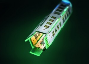
For operation in a 3D warning light in industrial plants, an HSMtec PCB is used which has to fulfill these requirements:
- Portable concept with remote control
- Simple installation process
- Reliable concept without cables
- Self-supporting PCB
- Direct PCB plug-in contact 1.6 mm thick
- Integrated thermal management
Discussion round as live chat
During the seminar, questions could be asked via live chat. This showed that the participants were mainly interested in individual PCB design requirements, such as the maximum copper thickness in the flex area or possible bending radii. The conclusion was that it always makes sense to involve the manufacturing company at an early stage when there are special requirements for the PCB so that an optimum design can be developed together without detours and setbacks.


