")
")
")
Dresden. Stretchable or even partially formable circuit carriers, miniaturization, high packing density, but increasingly also three-dimensionally assembled circuit carriers in the '3D-MID' process as well as better thermal management of densely packed systems are currently among the major trend topics in the PCB industry. This was the assessment of industry representatives and researchers at the 'Techvision 2024' symposium at the Fraunhofer Institute for Ceramic Technologies and Systems (IKTS) in Dresden. "Printed circuit boards are no longer just assembly carriers, but system carriers," emphasized Christian Ranzinger, Head of Technology at Berliner Contag, which co-organized the symposium. The driving force behind these developments is, of course, the desire of customers from automotive factories, mechanical engineering, medical technology, aviation and other sectors for greater functional density in the smallest of spaces. Just as semiconductor manufacturers use all kinds of 3D tricks to try to somehow continue 'Moore's Law' of ever-increasing integration depth under the motto 'More than Moore', a great deal of creativity is also required in PCB factories and from integrators in order to fill every cubic centimetre of empty space in the vehicle, aircraft or device with the additional electronics, sensors or actuators required. At the same time, however, it is also important to maintain a high level of quality, not exceed the thermal limits and prevent the circuits from dying of heat - a balancing act that requires innovative solutions. Thermal micromanagement for the circuit carriers is therefore increasingly becoming his main focus. One path that does not require a complete system replacement is the hybrid PCB, which is partly classically rigid, partly flexible or even windable. Where previously two different angled modules had to be connected by cables, which ultimately resulted in additional costs, potential sources of error and assembly times, such hybrids, including integrated circuits, adapt to the respective design in the device or vehicle.
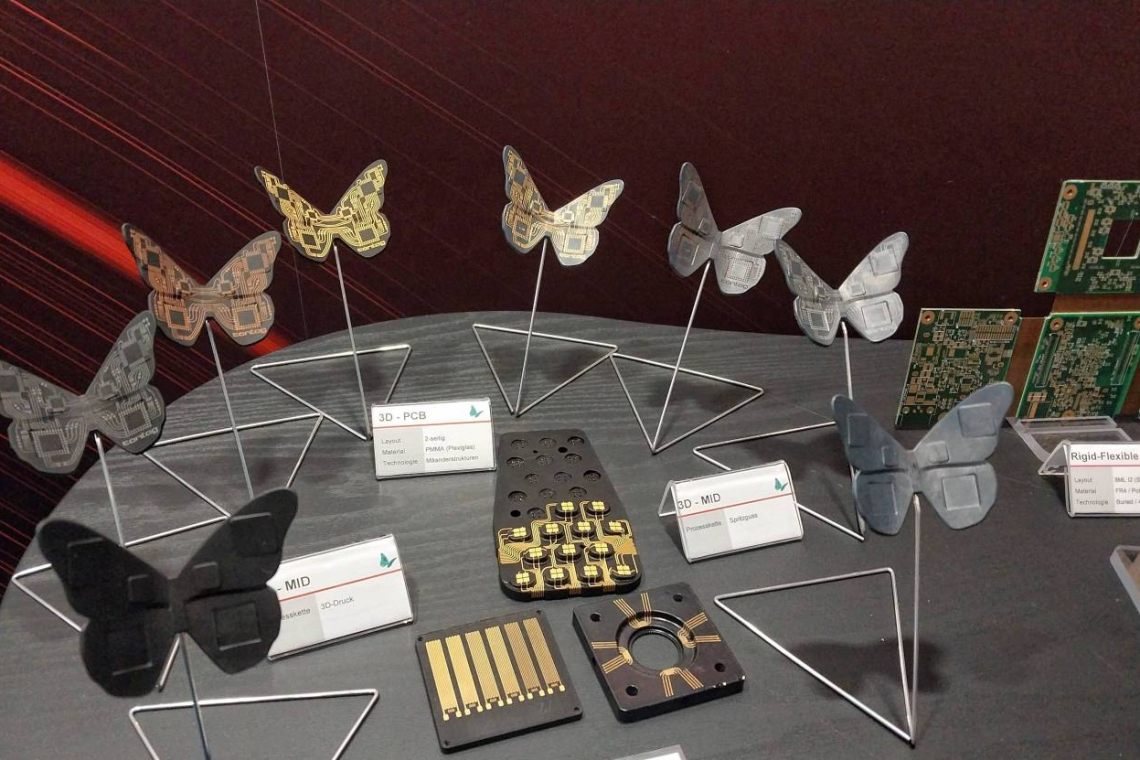
3D MID: The component itself is the circuit board
The '3D Molded Interconnect Devices' (3D MID) go much further: Here, the conductor tracks are integrated directly into three-dimensionally shaped functional components, usually produced by injection molding, for example recessed into the surface or plated through vertically and then assembled. To do this, manufacturers usually have to combine several production technologies that were previously not part of the repertoire of a traditional PCB company: plastic injection molding, 3D printing, laser drilling and structuring and the like. 3D-MID systems offer new prospects for electronic integration, particularly in automotive engineering, but also in medical devices, measurement technology and aircraft construction - wherever space is at a premium and digitalization is on the rise. At the same time, the combination of 'High Density Interconnect' (HDI) and 'Sequential Build Up' (SBU) is also gaining in importance in PCB technology if you want to achieve high-density circuits - according to one tenor at 'Techvision', which this year had the motto 'Electronics of the future - PCBs and beyond'. Multi-layer PCBs are produced in two or more sequential pressing steps, drilling and metallization. The drilling processes, the creation of buried contacts and the copper or resin fillings are central process steps and also place the highest demands on a high-precision production regime. Lasers are increasingly replacing mechanical tools as drills, as they allow smaller structure sizes of just a few dozen micrometers. In addition to greater packing density, higher reliability requirements are also playing a growing role for the industry: on-board electronics, for example, which have to withstand extreme fluctuations between very low and high temperatures or other harsh environmental conditions over years and decades. This applies to radar sensors in cars and high-frequency technology in satellites as well as level gauges and other sensors in various 'Industry 4.0' scenarios. Classic polymer circuit boards quickly reach their limits here, both due to the well-known plastic ageing and general stability limits. According to Dr. Steffen Ziesche from IKTS Dresden, ceramic circuit carriers can provide a remedy here: Low- and high-temperature single-fired ceramics (LTCC and HTCC respectively) therefore enable highly reliable and, if desired, truly hermetic enclosures; they are also particularly robust against mechanical and thermal stresses, emphasizes the research group leader.
'Cool' sintered ceramics open up new material options
Multi-layer 'Ultra Low Temperature Co-fired Ceramics' (ULTCC), which are sintered at temperatures of 'only' 400 to 700 °C, are particularly promising. This reduces the energy required for production. Above all, however, the relatively low sintering temperatures mean that far more functional materials can be used than in classic ceramic systems. "ULTCC components are ideally suited as rewiring carriers for electronic components, for housing and encapsulation technology or as substrates for high-frequency technology applications such as antennas, filters and circulators," says IKTS. Another advantage of ceramic circuit technologies: Their use can help companies to comply with the requirements of more recent environmental directives, for example by only using REACH-compliant materials. Dr. Christian Tschoban from the Fraunhofer Institute for Reliability and Microintegration (IZM) in Berlin highlighted the use of new packaging concepts (PCB) for the development of high-resolution and compact radar modules during 'Techvision'. One aim is to minimize the required antennas or to pack them particularly tightly. The IZM is pursuing several paths here. For example, the antenna technology can be realized as a monolithic microwave circuit (mmIC) in a cast wafer-level packaging (WLP), as a planar antenna on glass or as a 3D antenna in a compression molding process. A particularly large amount of space can be saved if antennas and chips are stacked three-dimensionally from the outset. In addition to such concrete application scenarios for advanced PCB technologies, the conference also focused on the phase between concept and series production. Contag's authorized signatory Dr. Frank Raspel outlined quick routes to prototypes and express PCBs - a particular speciality of the medium-sized company founded in Berlin-Spandau in 1981. Various processes continue to compete in the express sector. Recently, however, laser technology and additive manufacturing have been playing a growing role here.
Europe's largest ceramics institute as host
Following the presentations, the trade visitors were able to take a tour of selected laboratories, prototype workshops and production facilities at the research institute. With 40,000 m2 of floor space, three sites in Dresden and Hermsdorf and over 800 employees, IKTS is the largest ceramics institute in Europe. In addition to electronics and microsystems, the engineers, chemists, physicists and other specialists there work on new materials, high-temperature fuel cells, ceramic 3D printing, transparent and armored ceramics, innovative environmental technology and other key areas of research. For the business representatives, the choice of the Ceramics Institute as the venue was a sensible combination of two technology strands with a view to current challenges in the electronics industry. The high-caliber event brought together a wide range of experts on "forward-looking topics such as high-frequency transmission, new PCB technologies and ceramic circuit carriers", said Contag's Head of Sales Torsten Malsch. This provided a "platform for intensive networking and exchange between research and industry". In general, it should be noted that the local PCB industry plays an important role in the German and European economy. It generates an annual turnover of around 2.5 billion, is considered the backbone of the electronics industry and an important supplier for numerous other sectors. The industry is characterized by small and medium-sized companies, some of which specialize in niche markets and highly complex products. In an international comparison, the PCB industry in Germany enjoys a high reputation, especially from a technological point of view. German companies are particularly strong in high-frequency technology, high-speed printed circuit boards and special materials. However, German companies are under high competitive and cost pressure from the much larger PCB industries in Asia and especially China. For this reason, innovative technological approaches such as those discussed at 'Techvision' - such as 3D-MID and other high-integration technologies as well as ceramic circuit carriers - are likely to become even more important in the coming years in order to establish and expand unique selling points against the competition from China.
 Techvision 2024 was hosted by the Fraunhofer Ceramics Institute IKTS in Dresden
Sources:
Techvision, Contag, IKTS, IZM
