Christian Koenen GmbH from Ottobrunn successfully hosted its first Technology Day after the coronavirus-related break, demonstrating how the high precision required in fine-pitch stencil printing can be achieved.
 Michael BriandaMichaelBrianda, Managing Director at Christian Koenen, welcomed the participants, expressing his delight that such events with personal contact are now possible again, and then looked at the market situation.
Increasingly complex circuits combined with a high mix of designs and sizes and often thinner PCBs require smaller printing and assembly tolerances. The process window is getting smaller. The choice of materials and tools is of great importance for reliable precision printing. The paste volume can be optimized with stepped stencils. A coating on the stencil improves the release behavior and a PCB support during printing ensures stability.
PCB support is very important
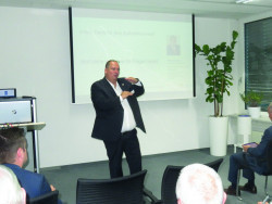 Michael ZahnBasedon the technology trends, Michael Zahn, Global Business Development Manager at Christian Koenen, explained how PCB support ensures error-free stencil printing. If the support is inadequate, bending and movement of the PCBs can cause solder bridges and beads as well as poor paste release, among other things. A large, rigid and firm support prevents this. He recommended a design with 3D software, as this follows the component contours, which ensures maximum support. Michael Zahn presented various application examples.
Milled step templates are one solution
 Sebastian BechmannAfterSebastian Bechmann, Head of Application at Christian Koenen, had explained what fine-pitch components are and the associated challenges, he explained how fine-pitch printing can be optimized. He showed examples of unevenness that disrupt the print. In addition, the substrate is often offset and the pad sizes are not suitable. Milled stepped stencils, a technique patented by CK, are often the solution here.
Semi-additive technology for the smallest structures
 Stephan DietrichStephanDietrich, Senior Process Engineer at GS Swiss PCB AG, presented the future of miniaturized PCBs and the possibilities of semi-additive technology. His company specializes in the production of miniaturized flexible printed circuit boards, e.g. for hearing aids. The trend here is towards L/S of 10µm and below, where conventional subtractive technology fails. He explained how such small structures can be realized with semi-additive technology and also showed photos of the equipment used. At GS Swiss PCB, the conductive layer required for electroplating is applied by sputtering.
Interferometry for measuring the smallest spatial structures
 Axel LindloffAxel Lindloff, Senior Process Specialist at Koh Young Europe, explainedhowthe smallest solder deposits can be measured automatically. 3D measurement with moiré interferometry is the industry standard. He described how this works in principle and how the measurements can be made more robust using phase shift profilometry. The phase shift also enables a very good height resolution. Lateral resolution is also important, especially for small structures. In addition, shadow effects must be reduced, which is possible with several projectors. Axel Lindloff showed examples from different areas of application, highlighting the precision that has now been achieved. The repeat accuracies are in the range of ± 0.1%.
The lunch break was followed by a company tour in small groups with subsequent networking in the Application Center.


