
The Bayerische Gesellschaft für Innovation und Wissenstransfer mbH (Bayern Innovativ) organized the Cooperation Forum for Printed Circuit Board Technology for the 17th time this year after the corona-related cancellation in 2021. Current topics and technological trends in the industry were discussed and practical application examples were presented in the Erding town hall.
As in previous years, Jürgen Frickinger, Bayern Innovativ GmbH, Nuremberg, officially welcomed the 120 or so participants and introduced the event. He introduced his organization and its diverse activities. Before presenting the agenda, he asked everyone the following question with regard to the next event: "Which key topics should be addressed at the next PCB Forum?"
Status and promising outlook
Hans Joachim Friedrichkeit, PCB-Network, Maulburg, began his look ahead with data on German PCB production. After steadily declining for many years, it grew again for the first time in 2021 due to restricted deliveries from Asia. The deglobalization that is now underway will continue to have an impact. Major growth markets for PCB applications are IC substrates and automotive technology. Friedrichkeit explained what the drivers are and how they will develop over the next few years (e-vehicles with a range of up to 1000 km, autonomous driving/ADAS level 4, matrix and laser headlights).
 Jürgen Frickinger
 Hans Joachim Friedrichkeit
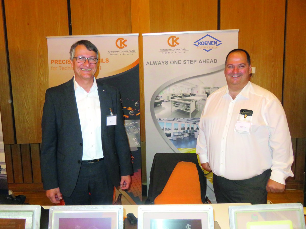
 Sven Johannsen
He then looked at the semiconductor market. The largest manufacturers are based in Asia, many American ones are fabless. More fabs are being built worldwide - in the battle for security of supply, especially in the USA and Europe. Construction of 29 fabs starts in 2022. The entire semiconductor supply chain is subject to change - including packaging, where system-in-package and system-on-chip solutions are becoming increasingly popular. The ABF substrates required primarily for high-performance CPUs/GPUs are not expected to be available in sufficient quantities for several more years due to the rapid increase in demand. On its way to becoming an all-in-one package, AT&S will significantly expand its production capacities for ABF substrates and thus enable even smaller structures (L/S up to 2µm in 2025).
 Pierre Lohrber
 Leon Haase
 Johann Hackl
Miniaturization with ultra-thin base materials
Sven Johannsen, Dyconex, Bassersdorf (CH), demonstrated that PCB miniaturization can be taken to the next level with ultra-thin base materials. He compared base materials on epoxy glass fabric with the woven and thinner ABF (Ajinomoto films) as well as structures with thin and thicker cores. The latter are more rigid and are well suited for assemblies with Ajinomoto films, which have advantageous properties for miniaturization and RF/HS signals.
However, continuous vias take up more space in these assemblies. In the semi-additive or additive process, smaller conductor pattern structures can be realized thanks to the thinner seed layer (without base copper). Johannsen showed examples of conductor structures realized in this way with L/S of 5µm. The solder mask must be adapted; thin solder masks such as those used on flex products are suitable. Due to the small structures, packaging applications also require new solutions for surface finishing, such as solder on pad (SOP). Using two application examples (6-layer structure for hearing aids and 6-layer structure for flipchip interposers), he illustrated the current state of the art and the challenges.
Before the lunch break, there was an exhibitor pitch session in which representatives from GulTech, KSG, Notion Systems, PCB Arts, Polar Instruments, Rogers and Varioprint provided information about their companies and their products.


Digital solder mask
One of the new additive manufacturing processes for printed circuit boards is the s.mask. Pierre Lohrber, Fela GmbH, Villingen Schwenningen, explained that the s.mask is the digital, additive revolution of the solder resist barrier. He compared the number of process steps and the results and possibilities of the s.mask with conventional solder resist masks applied by curtain casting. The advantages of the s.mask are: fewer process steps, targeted application/less material consumption due to not covering the entire surface, different layer thicknesses can be realized on one PCB, better edge coverage and filling of gaps, serialization/individualization by printing numbers and/or codes.
Now that the s.mask process has proven its strengths in the laboratory stage, it is being transferred to series production. Pierre Lohrber listed the associated challenges: Among other things, faulty or incorrectly calibrated nozzles can lead to unwanted conductor pattern wetting and there is an increased sensitivity of the s.mask to scratches under the influence of temperature. The process sets new standards, is sustainable and, above all, conserves resources.
 Andreas Folge
 Thomas Gottwald
 Lars Böttcher
High-current and thermal management
Johann Hackl, KSG Austria GmbH, Gars am Kamp (A), explained how high-current and thermal management can be realized with FR4 PCBs. He illustrated the different possibilities by comparing the technologies offered by KSG for high-current PCBs - these are thick copper, iceberg technology and HSMtec/embedding of copper parts. Based on the design principle, the performance was evaluated with regard to the following properties:
- high currents and very high currents up to over 150A
- Heat dissipation without heat sink
- Heat dissipation through the material to the heat sink
- freedom of design
- Possibility of combining high current and fine structuring
- Realization of different conductor cross-sections
- Further processability (assembly, soldering) and 3D capability
He then went on to discuss the influence of the ambient temperature and the layer structure as well as the design on the current carrying capacity and stated, among other things, as a guideline that the current carrying capacity of a conductor on a printed circuit board decreases by 5% for every 25K above 20°C/room temperature. Johann Hackl referred to the IPC-2152 guideline and the online high current calculator. A number of practical examples were used to examine solutions for thermal management and LED applications as well as the cost-benefit comparison of the technologies.
Laminates for 5G
Andreas Folge, Consultant Nan Ya Plastics Corporation, Bonn, provided information on laminates for high-tech requirements using the example of 5G. He began with a general introduction to the topic of 5G and explained what the product requirements associated with 5G mean for the base materials industry. Particularly low-loss materials are required for the millimeter waves. Resin, copper foil and glass fabric must be designed accordingly: The resin with the lowest possible polarity, the copper foil with lower roughness and a microstructure with few grain boundaries and the glass fabric with a low dielectric constant and spread (as uniform as possible). Nan Ya is the only base material manufacturer that does everything itself and offers a portfolio on this basis that also covers 5G requirements. Andreas Folge presented corresponding product solutions (selected for 5G) from Nan Ya. Further growth in the 5G market is expected in the coming years, combined with an increasing demand for corresponding base materials, which is why Nan Ya is continuing to invest heavily in this area.
SMD embedding
Leon Haase, Würth Elektronik GmbH & Co KG, Niedernhall, provided information on the technologies offered by his company for SMD embedding in series production. These are:
- Microvia.embedding: bare chips and special resistors and capacitors are mounted on inner layers or copper foils and the electrical contact is realized using microvias. The technology is suitable for maximum reliability and large series. Problems are caused by the availability of the components.
- Solder.embedding: SMDs are soldered to inner layers and the electrical contact is also realized in this way. The technology is suitable for high reliability and for small, medium and large series. The advantages are that no special components are required and existing processes are used.
- Flip-Chip.embedding: Bumped bare chips are mounted on inner layers and the electrical contact is realized by ICA (conductive adhesive). The technology is suitable for high reliability and for small, medium and large series.
Leon Haase explained the SMD embedding process in detail and also gave tips on the design. For example, a solder stop frame is always required around each mounting pad on the inner layer.
Embedding of power modules
Thomas Gottwald, Schweizer Electronic AG, Schramberg, described how power semiconductor embedding for individual power modules can be realized with maximum efficiency, using the example of p² Pack technology, the mass production of which will start this year. Embedding technology for power electronic components has many advantages in addition to miniaturization. These include higher efficiency, lower losses, greater reliability and improved heat dissipation. However, this requires semiconductors with copper connections and suitability for silver sintering or diffusion soldering as well as a high yield of 100% known good devices. After describing the structure and the resulting properties of the Smart p² Pack (MOSFET embedding), Thomas Gottwald presented examples with initial data for the High Voltage p² Pack and the Ceramic p² Pack, which are currently under development.
High-voltage power modules with SiC semiconductors
Following a detailed overview of the embedding technologies available for power modules from various manufacturers and the services offered by his institute, Lars Böttcher, Fraunhofer IZM, Berlin, provided information on the strategies for realizing high-voltage power modules with embedded SiC semiconductors. He discussed the design concepts with different insulator materials, the metallization of the semiconductor connections, the realization of heat dissipation (100W/chip) and the electrical design with the lowest possible induction as well as the selection of PCB materials. Lars Böttcher also described the process flow and the activities and previous results of the BMBF projects 'SiCModul' and 'SiCEffizient'. He then provided information on the AiF project '3D Power Electronics' for the integration of drivers and logic and the associated demonstrator concept with the idea of realizing a monolithic block with all functions. The highly informative event ended with a get-together.
