With IoT, AI and 'big data', the demand for functional electronics will increase many times over compared to today. 'Printed electronics' is seen as a way of using existing printing technologies to produce electronic components. Here is an overview of the current status and an outlook - the article is based on a presentation that the author contributed to the SGO Printed Circuit Board Seminar 2021 last September.
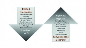
 Fig 1: Comparison of printed electronics with conventional electronicsIoT, AI and 'Big Data' will drive the demand for functional electronics much higher than it is today. Printed electronics' is seen as another way to manufacture electronic components - while using existing printing technologies. Here is an overview of the current status and an outlook - the article is based on a presentation the author contributed to the SGO PCB Seminar 2021 last September.
Printed electronics are made possible by advances in physics and chemistry: a wide variety of materials can now be formulated as inks with conductive/non-conductive and other required properties. Combined with modern printing techniques, this allows functional components to be printed. This is particularly interesting in areas where a large number of units have to be produced in a short period of time - think of a printed SARS-CoV-2 sensor, for example. In this way, daily testing of large population groups would be possible.
High-end applications that require short switching times and high densities would still be produced using conventional electronics. In addition, however, electronics can be created that serve the market for 'low-end' applications and can be correspondingly cost-effective due to the use of printing techniques(Fig. 1).
The foundations for printed electronics were laid at the end of the 1970s by the American Alan Jay Heeger (*1936), the New Zealander Alan Graham MacDiarmid (1927-2007) and the Japanese Hideki Shirakawa (*1936). They synthesized conductive plastics and were awarded the Nobel Prize in Chemistry in 2000 for their groundbreaking work in this field.
Immeasurable possibilities seemed to open up: printed solar cells, electronic paper, RFID antennas printed on individual products, sensors to monitor people's health and much more. In the end, however, it was not as simple as it initially seemed. Nevertheless, printed electronics has developed into a $30 billion market in recent decades (IDTechEx 2020). The largest item there is displays, the reason for this is that the major display manufacturers are focusing on oLED (organic Light Emitting Diode) materials and are increasingly using printing as a production technology. The next largest market shares are held by conductive inks and sensors.
Obvious similarities
If you compare PCB technologies in conventional microelectronics with printed electronics, you will see that they have a lot in common. Additive processes are used (electroplating in the PCB industry, printing in printed electronics), screen printing is used, flexible substrates can be used, multi-layer systems are realized and similar sintering and drying processes are used. The difference lies in the way in which structured conductor paths are generated. While photoimaging and etching processes are used in PCB technology, structures are applied in printed electronics using purely additive processes such as gravure printing.
Looking at the advantages of additive processes, one wonders why PCBs are not printed. There are several reasons for this:
The conductor paths in PCBs are based on continuous copper layers that are very good conductors. However, such a copper layer cannot simply be applied using a printer. Instead, an ink is used in the printer which consists not only of metal nanoparticles, but also a large number of other additives such as binders and dispersants, which are intended to guarantee 'printability'. After printing, the layer is heated so that organic additives burn off and the nanoparticles are sintered to form a conductive layer. Scanning electron microscope (SEM) images show that the result is not a continuous metal layer, but rather a network of interconnected nanoparticles.
Another problem is the copper itself: Copper nanoparticles oxidize very quickly; with printed copper you often have to make do with the much less conductive copper oxide. This is why the workhorse of printed electronics is silver - which in turn is much more expensive.
It is therefore unlikely that printed electronics will replace traditional PCB technology in the near future. Exceptions may be areas where simple, thin and flexible electrical components are required. These include membrane switches, touch panels, flexible heaters and RFID systems ('Radio Frequency IDentification'). The latter are highly interesting for industry and logistics in order to track goods easily and cost-effectively along the entire logistics chain.
Also worth mentioning in this context is so-called hybrid technology, in which conventional components are combined with printed conductive tracks, or 3D-MID technology ('Molded Interconnect Devices' or, more recently, 'Mechatronic Integrated Devices'), in which conductive tracks are integrated into injection-moulded plastic components. These can be applied using an aerosol jet printer, for example.
Where printed electronics can score
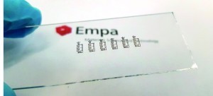
 Fig. 2: Silver electrodes for a ring oscillator printed with the aerosol jet printerButprinted electronics can score points with other advantages: for example, digital components can also be printed directly - with increasingly better performance in laboratory tests, but also in some products. A number of functionalities can be integrated into the printed element via an ink. The most advanced progress has been made in the field of electrochemical biosensors. Functional inks can be used to print layers that can detect an analyte via an electrochemical reaction. Printed glucose sensors, for example, are now ready for the market. Another example is screens: electrophoretic, electrochromic or even oLED materials can be printed directly onto a control board.
However, like many new technologies, printed electronics has also suffered some serious setbacks. One example is electronic paper, a screen technology based on the movement of charged black and white particles in a carrier liquid - all enclosed in small microcavities. Applied in a thin film to a flexible substrate printed with thin-film transistors, and you had an 'electronic paper': thin and flexible, with reflective contrast like paper, but electronically controllable like a computer screen, a revolution in the display market.
At the beginning of the millennium, several companies set about developing the product. The first prototypes were presented around 2005. But they were not a success. Polymer Vision with its Readius rollable display was scrapped in 2012, and PlasticLogic with its eInk display based on polymer thin-film transistors was also unable to bring a product onto the market for a long time. Only now, 21 years after the company was founded, does a change seem to be taking place and with Lectum a flexible display is being mass-produced.
Differences between graphic printing and printed electronics
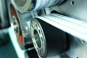
 Fig. 3: Often used for printed electronics: Roll-to-roll printing processLet's nowlookat the technical aspects: What steps does it take to move from print media skills to electronics? Firstly, you need functional inks, i.e. inks of conductive, semiconductive and/or otherwise functional materials. While a printed graphic is composed of individual printed dots (of different colors), the printed electronics must be able to produce defect-free layers.
If the pixel size of the print media is based on the resolution of the human eye, printed electronics only become interesting when it is possible to penetrate into the 20 µm range. For the printing of functional components such as a transistor, a high degree of overprint accuracy must be guaranteed in the printed electronics.
Simple printed electronic elements, e.g. an RFID antenna, are typically produced today using a screen printing process. A so-called functional paste is applied to a substrate through a fine-mesh fabric. For structured films, certain regions of the screen are closed with an emulsion. However, the possibilities of screen printing are limited. The resolution is limited to around 50 µm, the printing speed is rather moderate and a printing paste contains a very high proportion of binders and other additives in addition to the relevant functional particles.
Other printing techniques are therefore increasingly coming into focus for more complex components and structures. The digital printing techniques inkjet and aerosol jet are particularly popular in research and development(Fig. 2). Various geometries can be printed without great effort, the resolution reaches 20 µm with inkjet and even 10 µm with aerosol jet; another important aspect is the fact that these printing techniques can cope with relatively small quantities of starting material.
With a view to cost-effective mass production, the well-known high-resolution roll-to-roll flexographic and engraving printing processes are more interesting(Fig. 3), and so there are also many efforts to realize components here, even though the costs are much higher:
- it requires a solid understanding of the physics of the component
- the required base materials (e.g. conductor, semiconductor, dielectric) must be able to be brought into ink form
- the printing process as such must be understood, as this places high demands on the rheology of the ink.
This is explained here using engraving printing as an example. Gravure printing is a so-called gravure printing process. The areas to be printed are recessed in the printing form, typically a cylinder. Today, gravure printing is used in rotary printing presses for the production of magazines in large print runs and in packaging printing. During printing, the entire roller is inked and the excess ink is removed with a doctor blade. On contact with the substrate, a large proportion of the ink should be transferred to the substrate. Generally, an engraving cylinder is structured with cup-shaped indentations. In order to print a surface evenly, the drops transferred to the substrate must then melt into a continuous film.
If you take a closer look at the individual process steps, you will see that compromises have to be made in the ink formulation and printing conditions. When filling the cavities, air inclusions must be avoided, i.e. the cells must be able to be filled faster than the ink front moves (= printing speed). Low viscosity and high surface energy are decisive for this.
When removing the ink with the squeegee, another problem arises: the squeegee pulls ink out of the cavities and places the ink behind the cell. To suppress this process, the ink should be highly viscous and have a low surface tension. Another undesirable effect is the formation of a so-called 'smear film' which always forms between the doctor blade and the cylinder and then also leaves a thin film on the substrate. This may not be a problem in the graphics industry, but it is in printed electrical circuits.
As if that were not enough, the most important process, the transfer of the ink from the cavity to the substrate, is also subject to strict physical laws. A liquid bridge forms between the cavity and the substrate. Under the influence of surface tension and capillary forces, this bridge breaks open. The breaking point determines what proportion of the ink is transferred and what remains in the cavity. This should make it clear that even an ordinary color ink for engraving printing is a high-performance product. The increased requirements for functional inks for printed electronics make this even more challenging. Printed electronics benefit from the fact that the printing speed requirements can lag behind those of the graphics industry: The aim is to achieve print speeds of just over one meter per second.
Research and further development
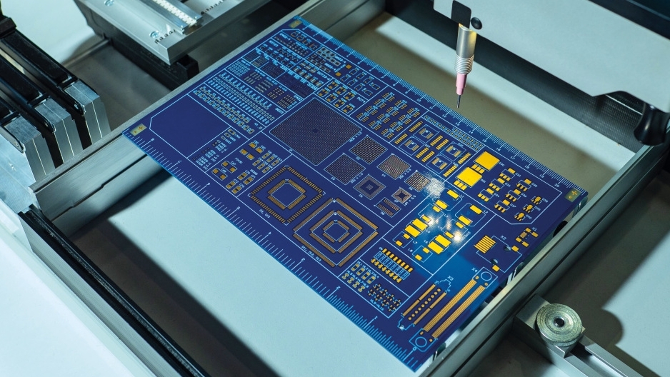
A number of universities, research institutes and companies are working in various areas of printed electronics. The Swiss Federal Laboratories for Materials Science and Technology (Empa), for example, houses a range of modern printing technologies at its Coating Competence Center in Dübendorf near Zurich(Fig. 4) and is addressing the most pressing issues in printed electronics. In current projects, transistors are being printed (https://www.sfa-am.ch/foxip.html) and the process steps in gravure printing are being optimized(https://www.sfa-am.ch/scalar.html).
It is definitely worth following the developments, as we can look forward to a range of printed electronics products.
 Fig. 4: High-precision printer from nsm Norbert Schläfli AG in a clean room at Empa's Coating Competence Center


