Electroplating plays a decisive role in the manufacture of printed circuit boards. Its main advantage is the reduction of the impedance of the line and the voltage drop. The process performance has a direct impact on the quality of the copper layer and the associated mechanical properties: In acid copper plating, the challenge is to achieve adequate layer thickness distribution and surface uniformity without unduly compromising metallurgical properties such as percentage elongation and tensile strength of the deposit. A reduction in current density can compensate for copper thickness to some extent, but will result in an excessive increase in overall plating time, which drastically affects the throughput of printed circuit boards. Therefore, proper control of the process performance and consequently the quality of the electroplated copper layer is an important part of PCB plating technology, which is one of the biggest challenges even for relatively experienced PCB factories. So it seems that early detection of the electroplating process performance in terms of copper layer thickness and distribution would add great value to proper process design and control. How can this be achieved? This is where the concept of a digital twin of the copper electroplating process comes into play.
Concept of the digital twin
A digital twin is nothing more than a virtual representation, the mirror image of a physical object, system or process. It is a digital counterpart that mimics the real entity in terms of its properties, behavior and interactions. The concept of the digital twin combines technologies such as the 'Internet of Things' (IoT), 'artificial intelligence' (AI), data analysis as well as modeling and simulation techniques (Fig. 1).
 Fig. 1: Concept of the digital twinDigitaltwins are usually created by collecting and integrating data from sensors, devices and other sources that are connected to the physical counterpart. This data is used to create a virtual model that replicates the physical object or system and allows it to be monitored, analyzed and optimized in real time. The digital twin can provide insights into the performance, condition and behavior of the physical object, enabling better decision making, predictive maintenance and performance optimization that can be developed in a safe and short period of time. The concept of the digital twin has applications in various fields, such as manufacturing, energy systems, healthcare, transportation and urban planning. In PCB manufacturing, for example, a digital twin can be used to analyze and optimize the copper plating process step by first identifying the actual process performance and then designing the optimal strategy to optimize performance.
The concept of the digital twin plays an important role in Industry 4.0 and smart manufacturing, which refers to the use of advanced digital technologies to create intelligent, connected and data-driven manufacturing systems (Fig. 2).
 Fig. 2: Industry 4.0 conceptDigitaltwins can play the following key roles in the concept of smart manufacturing:
- Design and development: digital twins enable manufacturers to create virtual prototypes of products and production systems. By simulating and analyzing different design options, companies can optimize product performance, shorten development time and minimize costs before physical production begins.
- Predictive maintenance: Digital twins help implement predictive maintenance strategies by analyzing the condition and performance of products and production systems based on engineering data and detecting early signs of potential failures. This enables proactive maintenance planning that minimizes downtime, reduces maintenance costs and improves overall equipment effectiveness.
- Optimization and simulation: Digital twins provide a platform for the simulation and optimization of manufacturing processes. By creating virtual replicas of production lines, the digital twin allows manufacturers to experiment with different scenarios, optimize workflows and identify opportunities to increase efficiency. This includes optimizing production schedules, minimizing energy consumption and reducing material waste.
- Product quality: Digital twins can monitor product quality throughout the manufacturing process. By integrating data from sensors and quality control systems, the digital twin can indicate deviations and causes of defects and suggest corrective measures. This ensures consistent product quality and enables traceability by capturing data on materials, processes and components used in the manufacturing process.
- Supply chain integration: Digital twins facilitate the integration and coordination of the entire supply chain in smart manufacturing. By creating virtual representations of suppliers, logistics networks and inventory systems, manufacturers can optimize material flow, inventory levels and logistics planning. This helps to reduce lead times, improve agility and increase overall supply chain performance.
- Continuous improvement and innovation: Digital twins provide a feedback loop for continuous improvement and innovation - by collecting data on product performance, customer feedback and market demand, manufacturers can analyze and identify areas for improvement. This includes optimizing designs, implementing product upgrades and tailoring offerings to specific customer needs.
All in all, digital twins in smart manufacturing enable data-driven decision making, increase operational efficiency, improve product quality and can drive innovation. They provide a holistic view of the manufacturing ecosystem and enable the optimization and continuous improvement of the entire value chain.
Concept of an electroplating process
In electroplating, a metal layer is deposited on a conductive surface through an electrochemical reaction. In the electroplating of printed circuit boards, the first step is an electroless process in which a chemical deposition of copper is applied to the surfaces of the printed circuit board, including the inside of holes. The purpose of this coating process is to create a thin metal layer on the PCB and in the holes, which serves as the basis for the subsequent electroplating process. The board is then prepared for the electroplating process:
- Impurities and drilling residues are removed from the holes
- The inside of the holes is subjected to a micro-etching process to improve the adhesion of the copper
- A photoresist is applied to both the top and bottom of the board
- The photoresist is selectively irradiated with ultraviolet light, leaving only the desired metallic circuit patterns unprotected
- The exposed and flexible photoresist covering the circuit patterns is washed off so that the remaining surface areas of the PCB are masked by hardened photoresist (Fig. 3).
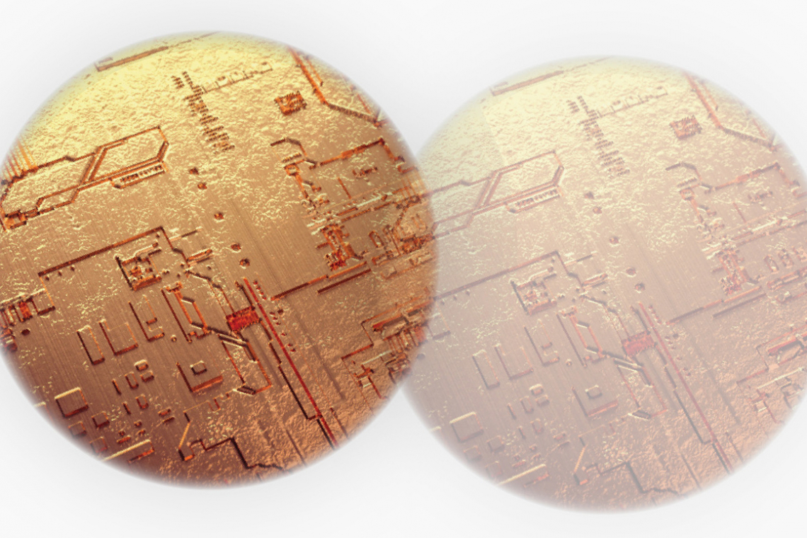
 Fig. 3: PCB manufacturing workflowAtthis stage, the PCB is prepared for electroplating with copper on the outer layers and in the drill holes. It is connected to the negatively charged cathode and immersed in a chemical bath specially developed for electroplating. During the electroplating process, the copper ions in the solution migrate towards the cathode and accumulate on the exposed copper circuits on the board (Fig. 4).
 Fig. 4: Schematic diagram of an electroplating process with highlights that influence the process performance
The copper plating process serves a dual purpose. Firstly, it increases the thickness of the copper on the surface pads and conductors, strengthening their integrity. Secondly, it establishes a reliable copper connection between the layers by extending through the plated through-holes. Thus, the quality of the electroplated copper layer directly affects the performance of the PCB as well as its mechanical properties and has a certain influence on the subsequent steps of PCB manufacturing. Therefore, the quality control of the electroplated copper coating is a crucial aspect of PCB plating technology, which is often a challenge even for experienced manufacturers. For example, they must take into account that problems associated with electroplating copper deposition can jeopardize the integrity of the connections in the hole walls, which can lead to possible failure of the PCB. One of the most common deposition defects is the presence of voids in the copper plating of the hole wall. Insufficient and incomplete plating of the hole walls can impede the flow of electrical current. The occurrence of voids in plated-through holes occurs when the copper is not coated evenly during the deposition process, which hinders effective plating. Several factors contribute to this, including impurities, the presence of air bubbles on the hole sides and rough drilling. These factors combine to create an uneven surface within the through-hole, making it difficult to achieve a seamless and uninterrupted copper layer. This challenge primarily affects PCB design, as through holes are an integral part of the PCB design. However, the design of the electroplating process and the lack of process control can cause further problems, the consequences of which can be seen in the uneven distribution of the copper layer. The challenges related to the process itself compromise the physical parameters(Fig. 4), which must also be considered: the type of electroplating bath and its electrochemical behavior, which depends on chemical composition and concentration, temperature, movement and current density; the substrate type, bath size, anode type, anode spacing and rectifier specifications. This already shows how many variables one needs to control to ensure that the copper electroplating process is operated in the most appropriate way so that uniform copper deposition can be achieved along all active surface areas on the PCB. Therefore, it seems reasonable and beneficial to use an approach that allows us to predict the distribution of electroplated copper layers on a specific PCB design before the actual physical process is set up. In this way, we can identify potential problems with uneven copper coverage and mitigate them in advance to ensure a reproducible process with the highest possible plating quality. The concept of the digital twin can be used for this purpose.
Performance evaluation of the copper electroplating process using a digital twin concept
A digital twin of copper plating is a virtual representation of the physical copper plating process as defined in the PCB manufacturing workflow. This involves creating a digital model that replicates the physical infrastructure of the electroplating process. This includes: Information about the copper bath (specifically the electrochemical behavior of the electrolyte represented by polarization data obtained from lab-scale deposition experiments), information about the electroplating tank infrastructure (tank dimensions, rack, anode types, anode-to-anode spacing and anode-to-cathode spacing, etc.), process parameters (deposition time, type of current program, etc.), and job data related to the specific PCB and board design(Fig. 5).
 Fig. 5: Digital twin for predictive modeling of electroplated copper layer distribution on a PCB - left: Digital twin data - right: simulation result - The color image shows differences in copper layer thicknesses: red color indicates too high layer thicknesses, while dark blue color indicates too low layer thicknessesBased onthis information, a calculation model is created and the analysis of electroplatability is performed based on the technology that uses finite element analysis (FEA) to solve the distribution of current density and calculate the metal layer thickness values using Faraday's law. The result of such simulations is a clear overview of the current density distribution and the distribution of the copper layer thickness across all active surface areas of the PCB product. Thus, the approach enables a pre-identification of all over- and under-coppered surface areas based on the PCB design and the setup of the electroplating line, taking into account the copper bath used. This in turn provides the opportunity to further optimize the process to achieve a more homogeneous distribution of the copper layers by further adjusting the process parameters (deposition time, current density) and/or developing a specific risk minimization strategy that affects the use of tooling components (shields, plating screens, blind plates, auxiliary anodes / conformal anodes; Fig. 6).
 Fig. 6: Copper plating simulation workflow using the 'Elsyca PCBPlate' software tool: Preliminary analysis of platability as a baseline simulation to identify the layer thickness distribution, design of a risk mitigation strategy - process optimization step, pre-validation of the improved process strategy - evaluation of the actual process performance after the preventive measures have been definedSinceboth process performance analysis and process optimization are performed in a computer environment, the predictive modeling or digital twin approach offers tremendous opportunities for better process design, analysis and optimization. It significantly reduces the number of tests for the wet process, saves resources at every level and ensures that the quality of the deposited copper layer always meets the requirements and is no longer dependent on the process operator. One of the biggest advantages of digital twins for electroplating is the ability to perform quick what-if analyses. With these, different scenarios can be explored to check the potential of the process for a variety of PCB products, from the rather simple to the most complex. This provides the opportunity to handle more jobs with different products from different PCB manufacturers.
The right copper balance in the design phase of a PCB
In PCB manufacturing, which includes etching and plating processes, copper traces are responsible for conductivity. Uniform copper plating on each PCB layer achieves uniform conductor thickness on the plated surfaces, which improves signal transmission and overall circuit performance. The homogeneous copper distribution across all active surface areas provides better PCB thickness during the lamination process and reduces the number of low pressure areas that may require redesign. Optimal copper coverage and thickness distribution during plating can be achieved by ensuring proper copper balance at the PCB design stage: Copper balance is one of the most important specifications to follow when manufacturing PCB products. It is used to achieve a symmetrical distribution of copper traces in each layer of the layer stack-up to avoid electrical and mechanical problems (curvature, twisting, deformation) that can affect the performance of the circuit. Looking at the electroplating process, an imbalance of copper on the top and bottom surfaces or within individual layer structures can lead to overplating, resulting in unwanted connections between traces or undercutting. A uniform layer thickness distribution is therefore important for several reasons:
- Current distribution: copper traces on a PCB conduct electrical currents between different components. When the current flows through a trace, it encounters resistance, resulting in a voltage drop. If the copper distribution is not balanced, some traces may carry more current than others, resulting in uneven voltage drops. This can lead to fluctuations in component performance and even circuit failure.
- Signal integrity: In high-speed digital circuits, signal integrity is critical to proper data transmission. Copper imbalances can lead to impedance mismatches and signal reflections that cause signal distortion, data errors and reduced system reliability. By ensuring copper balance, the impedance of signal lines can be controlled, minimizing signal degradation and improving overall system performance.
- Thermal management: Copper traces act as conductors for heat dissipation in PCBs. If the copper distribution is unbalanced, some areas may have a higher current density and consequently generate more heat. This can lead to localized hotspots that affect component reliability and performance. By balancing the distribution of copper, heat can be dissipated evenly, avoiding thermal issues.
- Manufacturability: Uneven copper distribution can affect the uniformity of etching and plating processes, leading to manufacturing difficulties and potential defects. By balancing the copper, the manufacturing process becomes more predictable and consistent, resulting in higher quality PCBs.
In most cases, however, copper balancing is often overlooked or inadequately performed in PCB design. This becomes clear when you look at user forums on PCB design. This is because copper balancing is usually done with standard PCB design software that provides predefined copper balancing options. However, relying solely on these built-in functions is not the optimal solution. These tools offer limited flexibility in defining the shape of copper areas and are often limited to selecting rectangular or polygonal objects from a predefined menu. In addition, copper balancing must be performed manually, which makes the entire process time-consuming. In addition, it should be noted that many copper balancing operations performed with common PCB design software fail due to incorrect specification settings and lack of understanding of the copper balancing approach. In Figure 7 you can see the consequences of inadequate copper balancing.
 – r.: Kurzschlüsse (rote Kreise), verursacht durch Lackrückstände, die nach dem Ablösen des Fotolacks im SES-Prozess noch eingeklemmt sind") Fig. 7: l. and m.: Front and back of a PCB design - improper copper balance in a standard PCB design tool resulting in overplated copper (red surface areas indicated by black circles) - r.: Short circuits (red circles) caused by resist residues still trapped after photoresist removal in the SES processTheimages on the left and in the center show overplated copper areas (marked in red inside black circles) on both sides of the PCB model (front and back). These overplated areas were the result of an incorrect copper balance during the design phase of the PCB. As a result, short circuits (marked with red circles in the image on the right) occurred due to resist residues that remained after stripping the photoresist in the strip-etch-strip (SES) process. These short circuits had a significant impact on the performance of the PCB.
Fig. 7: l. and m.: Front and back of a PCB design - improper copper balance in a standard PCB design tool resulting in overplated copper (red surface areas indicated by black circles) - r.: Short circuits (red circles) caused by resist residues still trapped after photoresist removal in the SES processTheimages on the left and in the center show overplated copper areas (marked in red inside black circles) on both sides of the PCB model (front and back). These overplated areas were the result of an incorrect copper balance during the design phase of the PCB. As a result, short circuits (marked with red circles in the image on the right) occurred due to resist residues that remained after stripping the photoresist in the strip-etch-strip (SES) process. These short circuits had a significant impact on the performance of the PCB.
To prevent the scenario described above, it is imperative that you follow the prescribed guidelines for proper copper balance:
- To avoid the formation of copper nests, it is crucial to distribute the traces as evenly as possible across the entire board. This principle should be followed for each individual layer, as well as for each axis of symmetry between two or more layers.
- If large areas are required, it is necessary to maintain the copper balance by symmetrically filling the corresponding layers with copper in the areas opposite the free areas. This ensures that there is a counterbalance to the copper in the opposite layer.
- Whenever possible, large copper areas should be laid out as a grid pattern. This grid structure helps to avoid bending or twisting effects, especially with single-layer PCBs. In addition, the use of a grid pattern promotes better uniformity of the copper along the walls of the plated-through holes.
To achieve the above objectives, a special copper balancing tool is used (see Fig. 8). It enables the PCB designer to optimize the copper balance by identifying critical areas on the PCB that could cause problems with the plating during the manufacturing process. By using an automated approach, potential problems can be effectively mitigated. The tool uses the Finite Element Method (FEM) to determine the balance area, which represents the copper density within each element in the balance area. This process ensures optimal copper distribution within seconds, with the result depending primarily on the complexity of the PCB design rather than the manual intervention of the PCB designer. Consequently, the tool allows for instant one-to-one comparison, facilitating design adjustments and reducing the likelihood that a redesign will be required.
 – r.: es sind keine Kupferkurzschlüsse (mit rotem Kreis markiert) zu sehen, da die Kupferbalance mit einem speziellen Elsyca-PCB-Balance-Softwaretool durchgeführt wurde") Fig. 8: l. and m.: front and back of a PCB design: correct copper balance leading to optimal copper thickness (marked with black circle) - r.: no copper shorts are visible (marked with red circle) as the copper balance was performed with a special Elsyca PCB balance software toolTheabove examples show that copper balance in PCB design ensures optimal power distribution, maintains signal integrity, promotes efficient thermal management and improves manufacturability. It contributes to the overall functionality, reliability and performance of the PCB and the electronic system of which it is a part. In addition, it has been shown that the right copper balance is a crucial step in achieving the desired copper thickness during electroplating. The concept of the digital twin enables a preliminary analysis and optimization of the surface treatment processes and the copper electroplating process of the PCB products. By virtually testing different scenarios and variables, manufacturers can determine the most efficient and cost-effective production parameters and avoidance strategies. This improves product quality, reduces scrap, shortens production cycles and increases overall productivity. Digital twins facilitate data analysis and performance evaluation. This data-driven approach supports continuous improvement initiatives and decision-making processes, and the virtual representation improves understanding, visibility and control over production operations, leading to long-term benefits.
Fig. 8: l. and m.: front and back of a PCB design: correct copper balance leading to optimal copper thickness (marked with black circle) - r.: no copper shorts are visible (marked with red circle) as the copper balance was performed with a special Elsyca PCB balance software toolTheabove examples show that copper balance in PCB design ensures optimal power distribution, maintains signal integrity, promotes efficient thermal management and improves manufacturability. It contributes to the overall functionality, reliability and performance of the PCB and the electronic system of which it is a part. In addition, it has been shown that the right copper balance is a crucial step in achieving the desired copper thickness during electroplating. The concept of the digital twin enables a preliminary analysis and optimization of the surface treatment processes and the copper electroplating process of the PCB products. By virtually testing different scenarios and variables, manufacturers can determine the most efficient and cost-effective production parameters and avoidance strategies. This improves product quality, reduces scrap, shortens production cycles and increases overall productivity. Digital twins facilitate data analysis and performance evaluation. This data-driven approach supports continuous improvement initiatives and decision-making processes, and the virtual representation improves understanding, visibility and control over production operations, leading to long-term benefits.
Translation: Markolf Hoffmann

Author
Agnieszka Franczak, PhD, heads the Surface Finishing Department at Elsyca, a provider of computer-aided engineering services for customers facing process design challenges. Franczak and her team develop special software solutions for electrochemical-based process analysis and optimization.
For more information:
www.elsyca.com,
References
[1] Elsyca PCBPlate solution: www.elsyca.com/elsyca-solutions/elsyca-pcbplatewww.elsyca.com/elsyca-solutions/elsyca-pcbplate
[2] Elsyca PCBBalance solution: www.elsyca.com/elsyca-solutions/elsyca-pcbbalancewww.elsyca.com/elsyca-solutions/elsyca-pcbbalance
[3] PCB Metal Balancing, patent, WO 2021/191346 A1.
[4] T. Lechler; J. Fuchs; M. Sjarov; M. Brossog; A. Selmaier; F. Faltus; T. Donhauser; J. Franke: Introduction of a comprehensive structure model for the digital twin in manufacturing, 25th IEEE International Conference of Emerging Technologies and Factory Automation (ETFA), 2020.
[5] G. Nelissen; B. Van den Bossche; I. Purcar; J. Deconinck: Three-dimensional simulations of current density distribution for patterned wafers and PCBs, In IPC, 2004.
[6] M. Purcar; B. Van den Bossche; L. Bortels; J. Deconinck; G. Nelissen: Three-dimensional current density distribution simulations for a resistive patterned wafer, Journal of the Electrochemical Society, 2004.
[7] G. Nelissen; B. Van den Bossche; L. Wanten: A performance simulaton tool for bipolar pulsed PCB plating, In ECWC 10 Conference at IPC, 2005.
Image sources
Elsyca
Sierra Circuits: www.protoexpress.com/kb/pcb-manufacturing-overview/
Acknowledgments
I would especially like to thank Sascha Reuter and Manuel Luschtinetz, Rohde & Schwarz, for providing reference materials for the copper balance simulations and the production results(Fig. 7 and 8) as well as for the excellent cooperation over the past months.
