Compared to various other light sources, light-emitting diodes (LEDs) stand out due to their long service life of up to 100,000 hours, low energy consumption, compact design and largely pollutant-free composition. Due to these outstanding properties, strong growth in LED technology is forecast for the global lighting market in the coming years. In future, ever more powerful LEDs (so-called high-power LEDs) will be used for applications where very high luminance levels are required. This is often the case when illuminating large outdoor areas, such as streets, squares, sports stadiums, industrial facilities and other infrastructure such as airports, railroad stations, railway tracks or port facilities. Sufficiently high heat dissipation via the metal core PCBs used is of great importance for the functionality of these high-power LEDs. The current state of the art is the use of epoxy resin systems as a dielectric (insulator) between the metal core and the conductor tracks. However, a major disadvantage of this synthetic resin is its very low thermal conductivity, which severely limits the power density and therefore the range of applications for high-power LEDs.
Compared with various other light sources, light-emitting diodes (LEDs) are impressive, among other things, because of their long service life of up to 100,000 hours, low energy consumption, compact design and largely pollutant-free composition. Due to these outstanding properties, LED technology is expected to experience strong growth in the global lighting market in the coming years. In future, increasingly powerful LEDs (so-called high-power LEDs) will be used for applications requiring very high luminance. This is often the case when illuminating large outdoor areas such as streets, squares, sports stadiums, industrial plants and other infrastructure such as airports, railway stations, railway tracks or port facilities. Of great importance for the functionality of these high-power LEDs is a sufficiently high heat dissipation via the metal core circuit boards used there. The current state of the art is the use of epoxy resin systems as dielectric (insulator) between the metal core and the conductor tracks. However, a major disadvantage of this synthetic resin is its very low thermal conductivity, which greatly limits the power density and thus the range of applications of high-power LEDs.
Basic structure of metal core PCBs
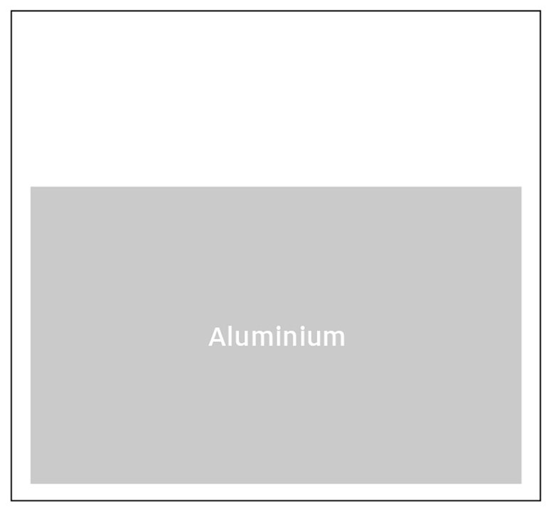
 Fig. 1: Schematic diagram of a metal core PCB for LED applicationsThebase body or carrier material of a metal core PCB is usually made of common, technical aluminum sheet material. This has a sufficiently high strength and can be easily machined and formed. Of particular importance for this application is the comparatively high thermal conductivity, which allows the waste heat generated by the LEDs to be dissipated efficiently.
A dielectric is then applied to this base material, which provides galvanic isolation between the current-carrying conductors and the metal core. Accordingly, this material must have a high electrical resistance or dielectric strength; an epoxy resin is often used for this purpose.
The conductive tracks are then applied to this dielectric in a multi-stage process. There are different variants, but basically the printed circuit board is first completely metallized in several steps (germination, electroless metallization, electroplating) and then subjected to a photolithographic process (application of photoresist, exposure, development, etching of the excess metallization) resulting in the desired conductor track structures.
Project objective
When considering the important thermal management of high-power LEDs, the epoxy resin used as a dielectric quickly turns out to be the bottleneck. This is due to the fact that the polymer has a low thermal conductivity of only approx. 0.20 W/(m∙K), which is typical for plastics.
As a result, the aim of this research project was to develop a coating system that combines the required properties, some of which are contradictory, such as good thermal conductivity, high electrical insulation and good adhesion of the conductor tracks. The basic idea was to replace the synthetic resin with a coating that also has a high electrical resistance but at the same time a higher thermal conductivity.
As aluminium is used as the carrier material and aluminium oxide has a thermal conductivity of around 28 W/(m∙K), which is around 140 times higher, anodization ("anodizing") was a possible coating process.
 a )
a )
 b )
b )
 c )
c )
Fig. 2: Schematic representation of the 2-stage anodized layer structure type "barrier layer"; a) Initial state, b) Step 1: Better adhesive strength due to large-pored and open-pored anodized layer, c) Improved dielectric strength due to reinforced barrier layer
Approach
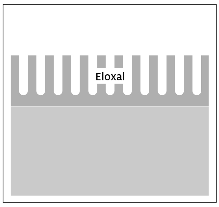
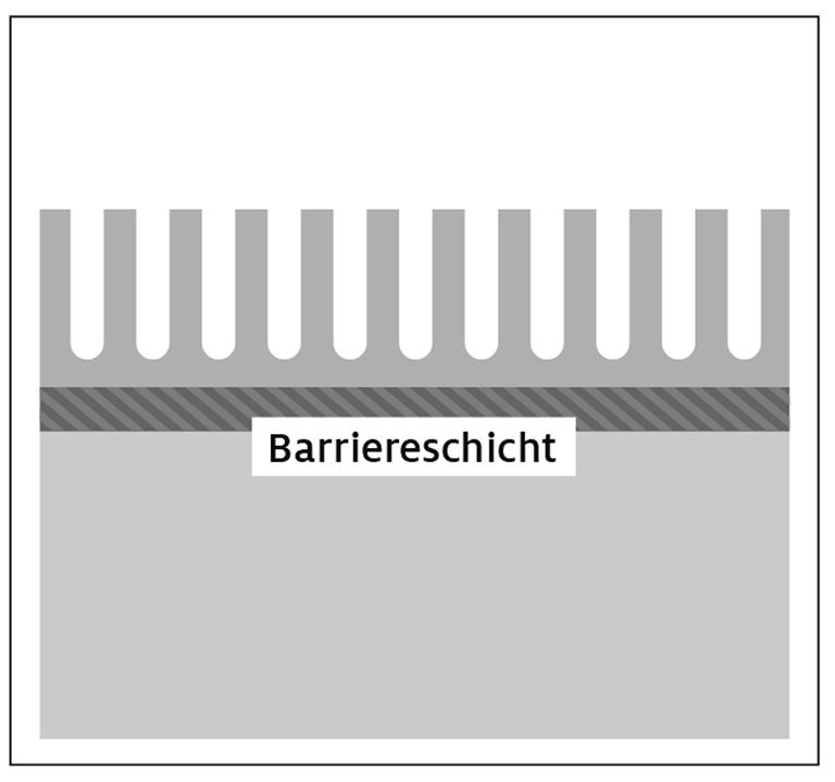
 des 2-stufigen Eloxal-Schichtaufbaus Typ „Sperrschicht“ (ohne Metallisierung). Im Bild unten das Aluminium-Grundmetall, oben die porige, unverdichtete Eloxalschicht, in der Mitte die auf rund 2 µm verstärkte Sperrschicht. Die Abbildung zeigt quasi den Idealzustand, welcher nur mit Reinst-Aluminium erzielt werden kann") Fig. 3: SEM image (cross-section) of the 2-stage anodized layer structure type "barrier layer" (without metallization). The picture shows the aluminium base metal at the bottom, the porous, uncompacted anodized layer at the top and the barrier layer reinforced to around 2 µm in the middle. The illustration shows the ideal state, which can only be achieved with ultra-pure aluminiumThemetallization of such anodized layers is not new, so it was known in advance that although this is possible in principle, it can also be associated with specific challenges depending on the specific application. In the present case, the requirements for high electrical resistance (dielectric strength) and good adhesion of the metallization (conductor tracks) were paramount. Preliminary tests have shown that these two requirements cannot be met simultaneously with conventional, single-stage anodized coatings.
Fig. 3: SEM image (cross-section) of the 2-stage anodized layer structure type "barrier layer" (without metallization). The picture shows the aluminium base metal at the bottom, the porous, uncompacted anodized layer at the top and the barrier layer reinforced to around 2 µm in the middle. The illustration shows the ideal state, which can only be achieved with ultra-pure aluminiumThemetallization of such anodized layers is not new, so it was known in advance that although this is possible in principle, it can also be associated with specific challenges depending on the specific application. In the present case, the requirements for high electrical resistance (dielectric strength) and good adhesion of the metallization (conductor tracks) were paramount. Preliminary tests have shown that these two requirements cannot be met simultaneously with conventional, single-stage anodized coatings.
Anodized layers have a characteristic (meso-)porous structure. A closed, non-porous barrier layer is only formed in the transition to the aluminum substrate, which is, however, very thin with a thickness of just a few nanometers. If such an open-pored anodized layer is metallized, very good adhesion can be achieved due to the intimate anchoring of the metal in the anodized pores. In this case, however, only the thin barrier layer is available as a dielectric, the resistance of which is nowhere near the required dielectric strength.
On the other hand, it is possible to compact the pores of the anodized layer. This can be achieved, for example, by simple immersion in boiling water, whereby the anodized pores are closed by increasing the volume of the layer. This allows thick, pore-free layers with sufficiently high electrical resistance or dielectric strength to be produced. Due to the absence of pores, nucleation only takes place on the surface, and the subsequently applied metallization has no possibility of interlocking with the anodized layer, which leads to insufficient adhesion.
The innovative approach of the project was to develop a two-stage layer structure that combines the respective advantages of the above-mentioned processes. Under the acronym "TwinEloxal", two different approaches were considered, namely the "barrier layer" type and the "compaction" type. Both have in common that the upper partial layer ensures good adhesion and the lower partial layer ensures high electrical insulation; however, the structure of these two layer systems differs significantly. In an extensive test programme, various influencing variables such as the alloy composition of the base material, type of pre-treatment, electrolyte composition and working parameters during anodizing were initially investigated on a laboratory scale, varied and optimized with a view to subsequent implementation on an industrial scale.
TwinEloxal "barrier layer" type
In this process, a conventional, relatively thick and large-pored anodized layer is first produced. For this purpose, typical pore-forming electrolytes based on sulphuric, oxalic or phosphoric acid were investigated, which differ in their layer properties, mainly with regard to the achievable pore diameters. In the second step, the thickness of the barrier layer is increased many times over. This is achieved by anodizing in a second electrolyte, which differs significantly from the first in terms of composition and working parameters. The so-called barrier layer-forming electrolytes are rather weak, mostly organic acids such as tartaric or citric acid, boric acid is also well suited for this purpose. As the thickness of the barrier layer depends directly on the anodizing voltage and increases linearly with it, relatively high voltages of several hundred volts are selected in this second step, although the resulting current density is very low.
 Erste Teilschicht mit großem Porendurchmesser, b) Zweite Teilschicht mit geringem Porendurchmesser, c) Schichtaufbau nach dem Verdichten") Fig. 5: Schematic representation of the 2-stage anodizing layer structure type "densification"; a) First partial layer with large pore diameter, b) Second partial layer with small pore diameter, c) Layer structure after densification
Fig. 5: Schematic representation of the 2-stage anodizing layer structure type "densification"; a) First partial layer with large pore diameter, b) Second partial layer with small pore diameter, c) Layer structure after densification
This layer system does not undergo any post-treatment in the form of compaction, so the upper partial layer remains open-pored, which results in good adhesion of the subsequent metal layer. Laboratory tests have shown that layers with very high electrical resistances can be produced under ideal conditions. The prerequisite for this is the use of ultra-pure aluminum, which is unsuitable for use in metal core printed circuit boards. However, the technical aluminium alloys used for this purpose have the decisive disadvantage that the intermetallic phases contained in this material are incorporated into the barrier layer or penetrate it and can thus cause undesired conduction of the electric current after metallization. For this reason, this approach was not pursued further in the course of the project.
TwinEloxal "compaction" type
This process also involves anodizing in two different electrolytes one after the other. Barrier layer-forming electrolytes are not used, but both partial layers are produced in pore-forming electrolytes. On the one hand, it is important that the upper layer has a larger pore diameter than the lower layer. Secondly, the system must be adjusted in such a way that the pores of the lower sub-layer are closed after the subsequent compaction process, while those of the upper layer remain open.
 des 2-stufigen Eloxal-Schichtaufbaus Typ „Verdichtung“ ohne Metallisierung (hier zur besseren Erkennbarkeit im unverdichteten Zustand). In der Übergangszone zwischen den beiden Teilschichten ist deutlich der Unterschied im Porendurchmesser erkennbar. Die untere Schicht lässt sich Verdichten, die obere bleibt auch nach dem Verdichtungsprozess offenporig und stellt somit einen guten Haftgrund für die anschließende Metallisierung da.") Fig. 6: SEM image (cross-section) of the 2-stage anodized layer structure type "compaction" without metallization (shown here in the non-compacted state for better visibility). The difference in pore diameter is clearly visible in the transition zone between the two partial layers. The lower layer can be compacted, the upper layer remains open-pored even after the compaction process and thus provides a good adhesion base for the subsequent metallization.
Fig. 6: SEM image (cross-section) of the 2-stage anodized layer structure type "compaction" without metallization (shown here in the non-compacted state for better visibility). The difference in pore diameter is clearly visible in the transition zone between the two partial layers. The lower layer can be compacted, the upper layer remains open-pored even after the compaction process and thus provides a good adhesion base for the subsequent metallization.
 des 2-stufigen Eloxal-Schichtaufbaus Typ „Verdichtung“ nach der Metallisierung. Auf dem Aluminium-Grundmetall (unten) befindet sich die untere, verdichtete Eloxalschicht (dunkler Bereich, Bildmitte). Die Metallisierung (heller Bereich oben) hat die obere, großporige Eloxalschicht in einem haftfesten Verbund durchsetzt, konnte jedoch nicht weiter in die verdichtete Schicht eindringen, welche somit ihre elektrisch isolierende Wirkung beibehält") Fig. 7: SEM image (fracture) of the 2-stage anodized layer structure type "compaction" after metallization. The lower, compacted anodized layer (dark area, center of image) is located on the aluminium base metal (bottom). The metallization (light area at the top) has penetrated the upper, large-pored anodized layer in an adhesive bond, but could not penetrate further into the compacted layer, which thus retains its electrically insulating effect
Fig. 7: SEM image (fracture) of the 2-stage anodized layer structure type "compaction" after metallization. The lower, compacted anodized layer (dark area, center of image) is located on the aluminium base metal (bottom). The metallization (light area at the top) has penetrated the upper, large-pored anodized layer in an adhesive bond, but could not penetrate further into the compacted layer, which thus retains its electrically insulating effect
 Fig. 8: Prototype of an LED module based on the TwinEloxal process type "compaction "Various electrolyte and thus layer combinations are possible, whereby anodizing in phosphoric acid has proven to be particularly suitable for the upper, adhesion-promoting partial layer, while sulphuric acid and, to a limited extent, oxalic acid are suitable for the lower partial layer to be compacted. As the laboratory tests showed good values for both the adhesion of the metal layer and the dielectric strength, this process was selected to be transferred to the project partners' industrial production facilities. The first prototypes were produced there as part of this project. The tests on these high-power LEDs based on TwinEloxal technology clearly show the desired, significantly improved heat distribution and dissipation.
Conclusion and outlook
The results of this project show that two-stage anodization can be used to produce anodized layers with tailored properties. Through the targeted variation and combination of working parameters such as pre-treatment, electrolyte, temperature, current, voltage and post-treatment, two-stage or multi-stage anodized coatings can be provided with extended or new functionalities and thus open up new areas of application. On this basis, the fem is currently conducting a research project on the production of adhesive, highly corrosion-resistant, galvanic coating systems on multi-stage anodized aluminium workpieces.
 Fig. 9: IR image of a conventional printed circuit board with epoxy resin as a dielectric. The color difference shows a large temperature gradient and thus an unfavorable heat distribution; the individual LEDs represent hotspots from which the heat can only dissipate poorly
 Fig. 10: The IR image of the newly developed metal core PCB with a 2-stage anodized layer as dielectric shows a significantly improved distribution and dissipation of the heat generated at the LEDs
Acknowledgements
The project "Development of an innovative multilayer anodized printed circuit board system for direct metallization for outdoor LED applications with high power density; development of highly insulating and adhesion-promoting anodization layers on a laboratory scale" (ZIM ZF4215101AG6) of the Research Association for Precious Metals and Metal Chemistry was funded by the Federal Ministry for Economic Affairs and Energy via the AiF as part of the Central Innovation Programme for SMEs (ZIM) on the basis of a resolution of the German Bundestag.
