At Laser World of Photonics 2022, the international photonics industry met again live in Munich from April 26 to 29, 2022. After the forced break due to the pandemic, the lasers shone again in the Munich exhibition halls. For the first time, the World of Quantum also provided a stage for the international quantum community.
In addition, the central role that photonics plays in medical technology, electromobility and industrial manufacturing, for example, became clear. The Fraunhofer-Gesellschaft was also represented at the trade fair with three joint stands. As part of a press tour, participants were able to find out about current research and development activities and applications. Selected stations are briefly presented below.
Miniature laser systems to search for traces of life in space
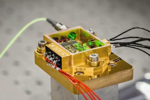 Fig. 1: The solid-state laser module built in Jena combines small size with maximum robustness (Photo: Fraunhofer IOF)
Was there life on Mars? The European Space Agency (ESA) wants to investigate this question with its ExoMars mission. Even though the launch of the mission planned for this fall is on hold due to current political developments, an interesting analysis system for use in space has been developed as part of the research work at the Fraunhofer Institute for Applied Optics and Precision Engineering IOF. The researchers from Jena developed a miniaturized laser module for the mobile laboratory of the ExoMars rover. The Raman spectrometer with a diode-pumped solid-state laser with frequency doubling is only the size of a 50-cent coin and weighs 50 grams including the housing (Fig. 1).
It can be used to examine the scattering of light on molecules in the atmosphere or on solids such as rock samples and to draw conclusions about the nature of matter from the changes in wavelength. The green laser from Jena operates at a wavelength of 532 nanometers and more than 100 milliwatts. All components of the sensitive laser resonator and the secondary optics were joined together using a laser-based soldering technique. The researchers now hope that their technology can soon be launched into space with the Mars mission(www.iof.fraunhofer.de).
Using lasers to combat microplastics
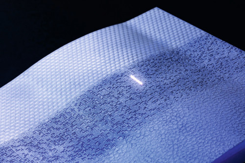
Until now, wastewater treatment plants have hardly been able to filter out the tiny microplastic particles in wastewater sufficiently. Now the first laser-drilled microplastic filter is being tested in a sewage treatment plant. It contains plates with extremely small holes just ten micrometers in diameter. The technology to efficiently drill millions of holes was developed at the Fraunhofer Institute for Laser Technology ILT (Fig. 2).
In the BMBF-funded "SimConDrill" project, the Fraunhofer ILT has joined forces with industrial partners to build a wastewater filter for microplastics for the first time. As part of the project, LaserJob GmbH drilled 59 million holes with a diameter of ten micrometres into a filter plate using a multi-beam process following process development at Fraunhofer ILT. An ultrashort pulse laser (TruMicro 5280 Femto Edition) was used for this purpose, with which holes could be drilled simultaneously with 144 beams. The special feature is that all partial beams can be individually controlled and therefore used to produce any surface structure. The aim is to increase the speed of the process by a factor of twenty to fifty and thus significantly increase the cost-effectiveness of the process.
Optical coherence tomography for more stable and safer laser processing
In laser processes, deviations in the parameters of the laser quickly lead to serious defects in the component, which is why it is important to react immediately. The Fraunhofer Institute for Production Technology IPT in Aachen has developed a modular system based on optical coherence tomography (OCT), which can be used to detect deviations during laser processing (Fig. 3).
OCT is a non-contact measurement method that can provide high-resolution two- and three-dimensional images of semi-transparent materials. With its high measuring frequency of several kilohertz, OCT also makes it possible to measure the surface distances of opaque technical components with extreme precision. This allows the condition of workpiece surfaces to be checked during an ongoing production process. This is particularly advantageous for laser processing, as it allows the company to react to changes in the process in real time.
The OCT system is integrated into the processing module coaxially, in a common beam path with the laser. The laser and the OCT system use the same optics - but at different wavelengths. This saves space and the installation costs of additional expensive optics and allows measurements to be carried out directly in the process. The laser machining process is not affected by the measurement and any number of measurement patterns can be defined.
Hiclad ensures resilient laser metal deposition with high-power lasers
High-power diode lasers with outputs of ten kilowatts and more open up new application scenarios for laser metal deposition. Together with partners from industry, the Fraunhofer Institute for Material and Beam Technology IWS has now developed applications and specific processes under the Hiclad label for this class of industrial lasers to practical maturity. A core element of the Hiclad family is the innovative COAXquattro laser cladding head. A laser beam runs through the center of the nozzle, around which up to eight separately controllable channels feed powder and wires.
For the first time, COAXquattro enables the simultaneous processing of powder and wire in various combinations. The materials meet in the laser focus above the component surface, where the laser melts the supplied metal. The coating is created in-situ directly on the surface from the powder and the individually fed wires. In contrast to powder-based deposition welding, wire-based processes were previously limited to a maximum of six kilowatts. With COAXquattro, it is now possible to use laser powers of up to 20 kilowatts in the combination of wire and powder, and the next step will lead to the 45-kilowatt class The technology was presented at the joint Fraunhofer stand.
Inline-capable 100% spectroscopic inspection for industrial quality assurance and process control
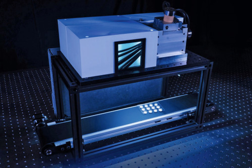
Companies in the pharmaceutical, chemical and food industries depend on meeting the highest quality requirements and optimizing production processes at the same time. In collaboration with the Fraunhofer Centre for Applied Photonics, Fraunhofer IAF has developed an integrable measuring system for such applications that uses machine vision to specifically detect samples and verifies them contact-free within a few milliseconds using laser-based infrared spectroscopy. Contaminated or incorrectly assembled specimens can thus be sorted out immediately (Fig. 4).
The specific advantages of the system result from the backscattering spectroscopy method in the mid-infrared with wavelengths in the range of 4 to 12 μm. As molecular compounds have very characteristic absorption and emission lines in this spectral range, they can be clearly identified. One of the core components of the measurement system is a broad-emitting and spectrally fast scanning laser module, a combination of quantum cascade laser and micro-opto-electro-mechanical grating scanner. To illustrate the integration capability of the measurement system in industrial processes, the Fraunhofer IAF team has developed a practical demonstrator, which was presented at the trade fair.
Highly sensitive quantum magnetometers on their way into industry
Fraunhofer IAF also presented a quantum magnetometer based on diamond. It is designed to detect magnetic fields with a spatial resolution of a few nanometers down to individual electron and nuclear spins. Due to the physical properties of the material, diamond quantum magnetometers work at room temperature, which is ideal for industrial applications (Fig. 5).
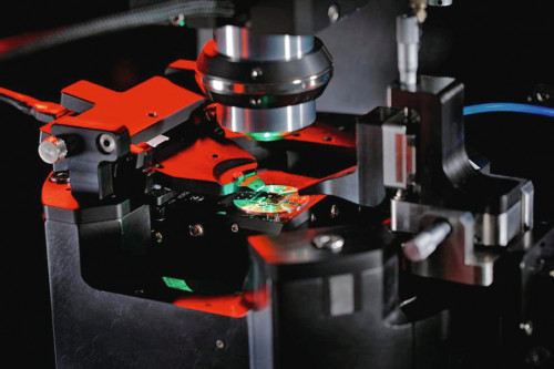 Fig. 5: In the quantum sensor application laboratory at Fraunhofer IAF, partners from science and industry can evaluate quantum magnetometers for their specific requirements
Fraunhofer IAF also presented a quantum magnetometer based on diamond.
Fraunhofer researchers from six institutes have joined forces in the project "Quantum Magnetometry" (QMag for short) to develop, among other things, an imaging scanning probe magnetometer based on nitrogen-vacancy centers (NV centers) in diamond for the most precise measurements of nanoelectronic circuits. Great progress has already been made in the development and optimization of diamond sensor tips. This concerns both the growth of high-quality diamond and the targeted generation and placement of NV centers in the diamond tips. In addition, the researchers have developed microlenses and synthesized magnetic nanoparticles that are introduced into the diamond tips in order to further optimize them in terms of accuracy and efficiency.
Optical housings for encapsulating components
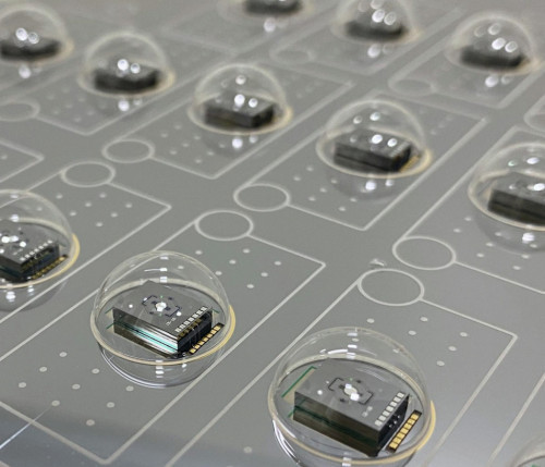 Fig. 6: Substrate wafer equipped with scanner mirrors, the encapsulation of the components is realized here with a glass lid wafer (Photos: Fraunhofer ISIT)
With the integration of optical functions in microsystems, the packaging of components and systems at wafer level (WLP) is facing new challenges (Fig. 6).
A process developed at the Fraunhofer Institute for Silicon Technology ISIT enables the production of precise optical components at wafer level for various applications at low cost. If the silicon wafer is provided with structured recesses, the glass can be molded into these embossed structures. The resulting glass structures are then exposed by dissolving the original silicon wafer in a lye bath.
The surfaces of glass molds produced in this way are created without material contact and are therefore flat, with roughnesses of less than one nanometer, a must for optical applications. In this way, optical components such as lenses, concave mirrors or domes of high optical quality have been produced from glass at Fraunhofer ISIT. As these shapes are produced on wafers, a large number of optically identical components are always produced simultaneously, resulting in low production costs(www.isit.fraunhofer.de).
MEMS scanners for wide-angle LIDAR systems
LIDAR (Light Detection and Ranging) is an indispensable key technology in the development of self-driving cars. LIDAR systems use emitted laser beams to detect their surroundings very accurately and generate a precise image. However, their resolution is significantly higher than that of radars, which makes this technology so indispensable, because the more precise the image, the better the on-board electronics of the self-driving vehicle can react.
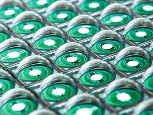 Fig. 7: MEMS scanners encapsulated with glass domes for LIDAR applications
Until now, LIDAR systems have been very large and very expensive, which has made them difficult to use in vehicles. This is why Fraunhofer researchers are now trying to develop small, cost-effective and high-resolution LIDAR systems whose manufacturing costs do not stand in the way of commercialization in the automotive industry. In principle, such a system consists of a laser, a scanner that emits the laser beams and a capture optic that reads the reflected laser beams. The individual components communicate with each other via suitable electronic interfaces.
Finally, a dome-shaped glass cover was mounted on the MEMS mirror, a pioneering, innovative development from Fraunhofer ISIT. This glass dome protects the component from environmental influences and ensures the good optical quality of the component. Fraunhofer ISIT showed the MEMS scanner at the Fraunhofer booth.


