During component coating already deposited particles are incorporated into the growing layer and continuously deposited on the surface. There a characteristic defect growth structure is formed, which is reflected in a particle surface as well as a roughness. In this work, it is shown that the production of doped carbon films using composite cathodes leads to a significant reduction in arc-induced particle emission. While Part 1 covered origins of growth defects, methods of surface characterization, experimental setups and measurement methods, the final part of the article delivers the measurement results and highlights the conclusions.
Results and Discussion Coating Properties
Results of coating thickness measurement, chemical composition and mechanical analysis of the coating are shown in Table 1. Values for coatings of around 1 µm thickness and around 5 µm are analyzed. Coatings with non-metal dopants (B, Si) are referred to as ta-C:X, because of the near-ta-C behavior especially in terms of mechanical properties, like hardness or Young’s modulus, whereas metal dopants (Fe, Mo) lead to the formation of softer a-C:X coating. This behavior is known from several studies [3, 8, 29–32]. After the deposition process for all coatings the chemical composition is analyzed. Compared to the nominal dopant in the cathode (for all cathodes 5 at. %), the amount of dopant, except of Boron, is increased in the coatings.
|
Target |
Resulting coating |
Amount of dopant [at %] |
Coating thickness [µm] |
Indentation hardness [GPa] |
Young’s modulus [GPa] |
|
C (pure) |
ta-C |
– |
0.9 ± 0.2 |
52.2 ± 0.8 |
526 ± 13 |
|
– |
4.9 ± 0.4 |
52.5 ± 0.9 |
541 ± 15 |
||
|
Non-metal dopant |
|||||
|
C-B |
ta-C:B |
4.7 |
1.6 ± 0.2 |
48.6 ± 1.4 |
528 ± 15 |
|
5.0 |
4.2 ± 0.3 |
50.9 ± 0.5 |
530 ± 9 |
||
|
C-Si |
ta-C:Si |
5.7 |
1.0 ± 0.2 |
41.9 ± 0.7 |
436 ± 8 |
|
5.7 |
4.3 ± 0.4 |
44.8 ± 0.2 |
497 ± 5 |
||
|
Metal dopants |
|||||
|
C-Fe |
a-C:Fe |
10.2 |
1.1 ± 0.2 |
12.4 ± 0.2 |
162 ± 4 |
|
10.3 |
4.0 ± 0.4 |
14.4 ± 0.1 |
168 ± 4 |
||
|
C-Mo |
a-C:Mo |
6.4 |
0.8 ± 0.3 |
15.3 ± 0.4 |
228 ± 8 |
|
7.4 |
4.9 ± 0.5 |
25.2 ± 0.3 |
323 ± 5 |
||
SEM analysis of surfaces and cross sections
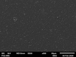
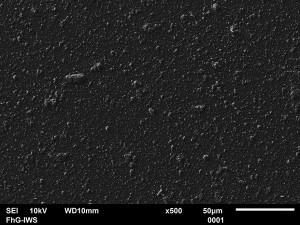
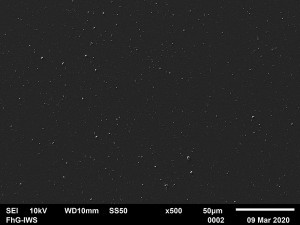
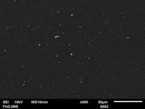
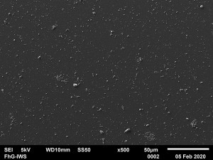
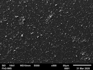
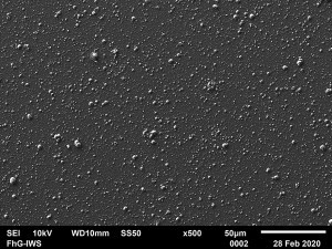
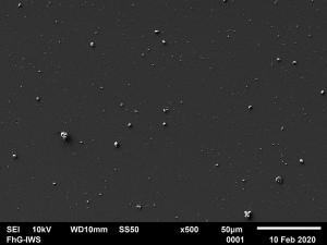
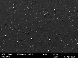
Increasing the coating thickness normally increases the surface defect fraction in ta-C, which is common for all PVD-coatings as stated in Sec. 1.1. SEM examination of the coating surfaces shows this effect qualitatively in Figure 1 for undoped ta-C and doped (t)a-C:X. Remarkably, for thinner coatings (Fig. 1, left column, 1 µm), the surface defect fractions for ta-C is already very high in comparison to the doped coatings. However, there are differences between the doped coatings. Comparably large surface defects are found for ta-C:Si and a-C:Mo, while ta-C:B and a-C:Fe have many smaller defects. If the coating thickness is increased up to 5 µm (Fig. 1, right column), the surface defect fraction for ta-C:B and a-C:Mo is significantly lower than for the other types of coatings, but there are clear differences in the growing behavior of the defects depending on the coating type. For ta-C the surface defect fraction increases drastically, showing many large and even agglomerated defects. The ta-C:Si and a-C:Fe show a similar increase of the surface defects. Only for ta-C:B and a-C:Mo the growth of the defects is rather different, leading to smooth surfaces even in thicker coatings. The reasons for these differences are not yet understood and objects of current research. For better understanding of the evaporation process and the initial particle formation it would be useful to quantify this surface defect fraction. For this reason and to quantify this surface effect, the surface characterization method, described in Sec. 2.3 was developed and utilized.
Fig. 1: SEM surface images of undoped and doped carbon coatings with coating thickness of about 1 μm and 4–5 μm
In order to investigate the homogeneity of the coatings, cross sections of each coatings were prepared by cryo-cracking the samples. Figure 2 shows an ensemble of cross section of all coatings for a coating thickness of about 5 µm. Whereas ta-C shows a very inhomogeneous cross section with features and many holes of former particles and their growth products, the doped coatings seem to be smoother not only on the surface but also in the cross sections. Exceptions are ta-C:Si and a-C:Fe, showing a heavily covered surface. Non-metal dopants lead to very smooth and unstructured almost glassy cross section. Using metal dopants, the cross section is more structured and has a rough appearance.
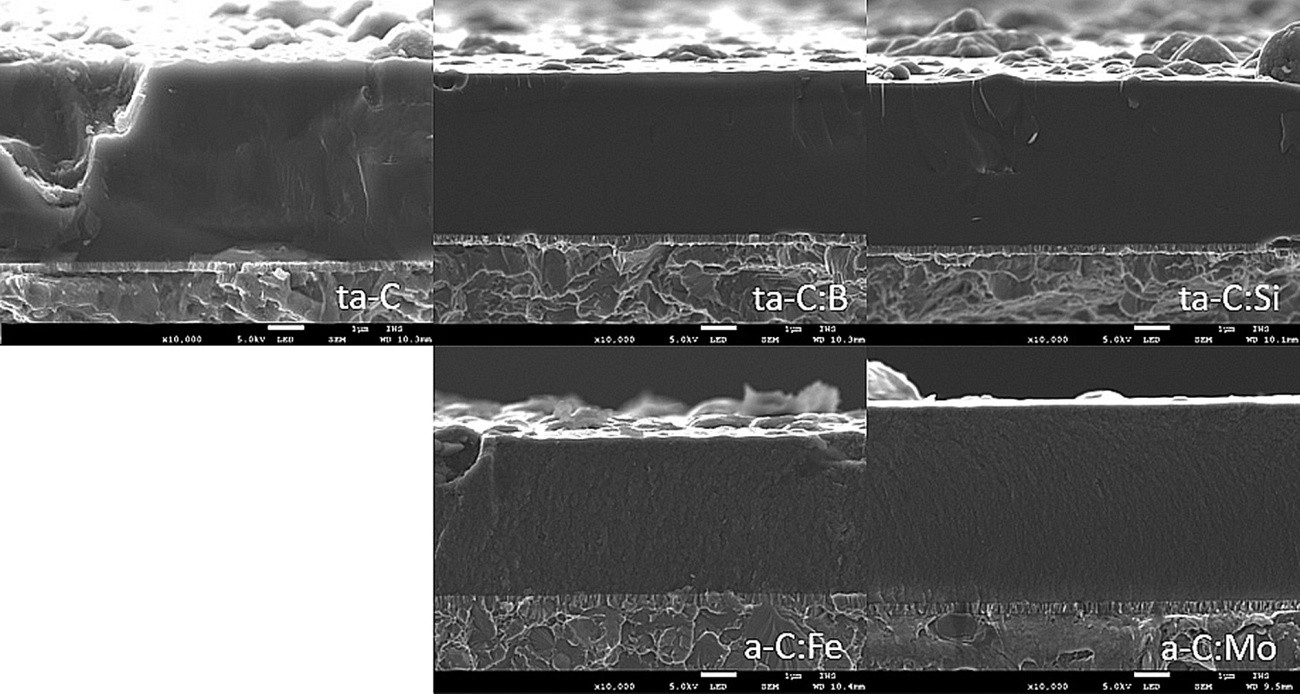 Fig. 2: Cross sections prepared by cryo-cracking of undoped and doped carbon coatings with coating thicknesses of 4–5 μm
Correlation of surface defects, roughness and coating thickness for undoped ta-C
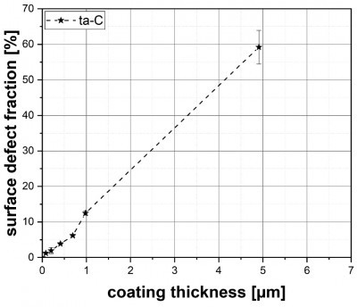 Fig. 3As mentioned above, the incorporation of macro particles into the growing ta-C film leads to the formation of cone shaped nodular growth defects. Analyses via digital image processing detect the growth defects and the defects visible on the surface, and subsequently evaluate the surface defect fraction. This parameter describes thus the proportion of the area covered with growth defects or incorporated particles. Due to the continuous formation of new growth defects and their conical growth during the deposition process, the surface defect fraction is strongly correlated with the deposited coating thickness. To demonstrate this dependency, several ta-C coatings were deposited by Laser-Arc-deposition. The microscopic images in Figure 3 a–f show the surface of the deposited ta-C coatings at increasing thickness up to a maximum of 5 µm. It can be clearly seen that even at thin films of ~0.8 μm a certain amount of growth defects is initially present in the coatings. With uniform buildup of the ta-C film these defects continuously grow in size and some defects grow together as agglomerates. Furthermore it can be observed that new particles are generated throughout the deposition process, forming smaller growth defects, when incorporated into the growing film. If the surface defect fraction is considered as a function of the film thickness, as shown in the diagram in Figure 3, a linear relationship between these two parameters could be approximated. Regarding these unfiltered ta-C coatings, the proportion of the area covered with growth defects shows a very rapid increase at steady film growth, so that at a thickness of 5 μm, already more than 50 % of the surface is covered with surface defects. This may indicate a high emission rate of carbon particles from pure carbon targets during the arc evaporation process.
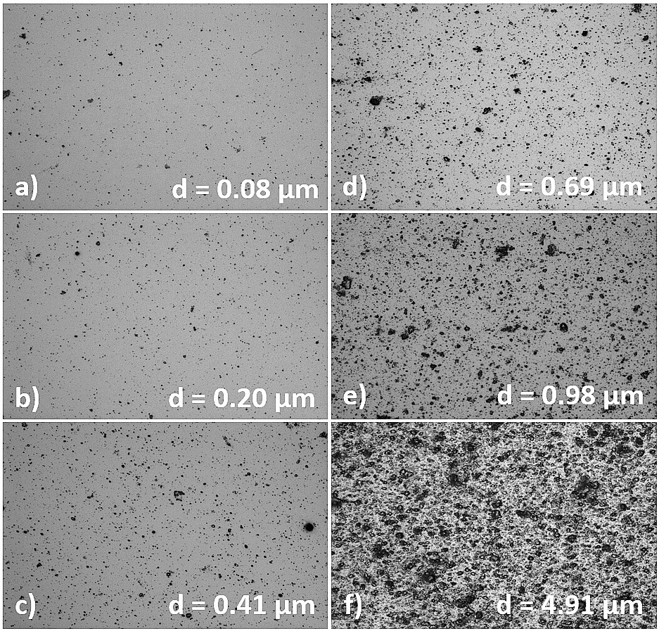 Fig. 3: Surface defect fraction (particle coverage) as a function of deposited thickness on ta-C coatings and light microscope images of the corresponding surfaces with absolute coating thickness values (a–f)
The high defect fraction of ta-C coatings also reveals the limits of the surface defect characterization method. The standard deviation of the measured values gets to a non- acceptable level above a growth defect fraction of about 50 %. Here, the threshold in the histogram (Fig. 4b, GT 3-2021, S. 316) can no longer be set correctly and it gets difficult to distinguish between the growth defects and the background. It was thus determined that the measurement procedure for evaluating the growth defect density guarantees suitable results up to layer thickness of 5 μm or surface defect fractions up to 40 %.
![Fig. 4: Surface roughness (described by Ra value) of ta-C coatings as a function f deposited coating thickness compared to literature [2] Fig. 4: Surface roughness (described by Ra value) of ta-C coatings as a function f deposited coating thickness compared to literature [2]](/images/stories/Abo-2022-04/gt-2022-04-0047.jpg) Fig. 4: Surface roughness (described by Ra value) of ta-C coatings as a function f deposited coating thickness compared to literature [2]
Fig. 4: Surface roughness (described by Ra value) of ta-C coatings as a function f deposited coating thickness compared to literature [2]
The total amount and size of the growth defects on the surface significantly affects the surface roughness of the coatings. This is usually expressed by the Ra values, acquired by the analyses of optical or tactile interferometry. In Figure 4 the tactile Ra values are illustrated as a function of the growth defect density to show the mutual correlation of these values. Similar to the surface defect fraction a linear correlation to the deposited coating thickness can be assumed. This assumption is further confirmed by recent investigations on the influence of doping concentrations on the coating properties of ta-C coatings by Schulze [2], as demonstrated in Figure 4.
In addition to the film thickness influence, a clear effect of the dopant elements on the defect fraction can be observed. Figure 5 shows the surface defect fraction as a function of the deposited coating thickness for the different doping elements. It can be seen that all analyzed doping types lead to a significant reduction of the surface defect fraction compared to pure ta-C coatings at a coating thickness of 4–5 μm. The lowest values were achieved by doping ta-C with B and Mo, which decreases the surface defect fraction by about an order of magnitude from 59 % for pure ta-C to 6.5 % for Mo and to 5.3 % for B, respectively. Up to 1 μm all doping types except Si exhibit similar (low) surface defect densities when incorporated into ta-C coatings. The effect of Si is only pronounced at the thicker coatings where it causes a reduction to one third of the initial value for ta-C.
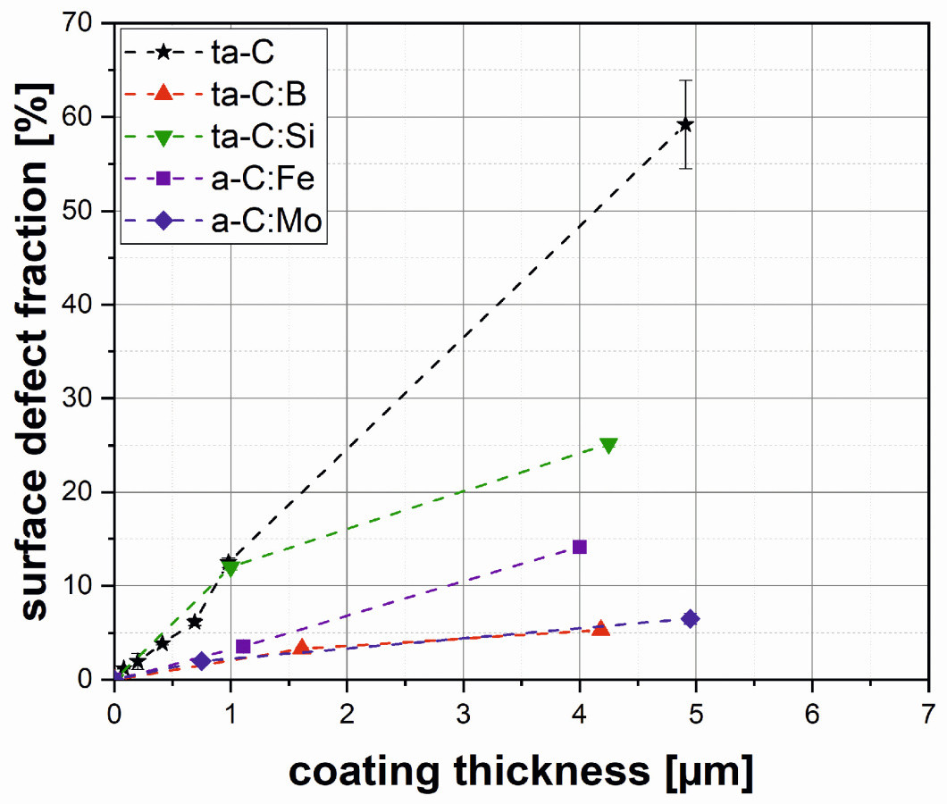 Fig. 5: Surface defect fraction as a function of coating thickness for ta-C and different dopants
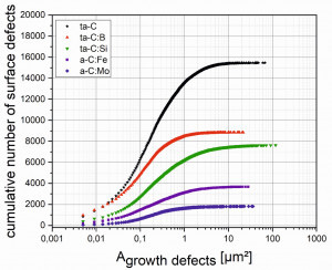
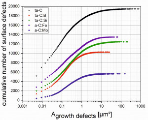
The a-C:Fe coatings exhibit similar values at thin 1 μm coatings as a-C:Mo and B, but show a faster increase at thicker coatings, where about 14 % of the surface is covered with surface defects at a film thickness of 4 μm. In order to examine the effect of the doping elements in detail, the cumulative number of surface defects over the respective defect size for each coating type is shown in Figure 6.
Figure 6a and 6b refer to the 1 µm and 4–5 µm thick coatings, respectively. In both diagrams the highest number of growth defects is recorded for pure ta-C. At a thickness of 1 µm all coatings show a similar distribution of very small defects at the size of 0.005–0.01 µm2. However, pure ta-C exhibits a very steep gradient at larger defects of up to 1 µm2, indicating that many of them are present on the surface. Contrary, 5 µm ta-C coatings already show a significant higher number of small defects while the gradient remains similar in all investigated coatings. All doped coatings show a lower number of defects at 1 µm as well as on the 5 µm thick coatings. Among the doped coatings, ta-C:B exhibits the most defects on the surface at 1 µm, followed by ta-C:Si and a-C:Fe. At a coating thickness of 5 µm, however, both elements (Si and Fe) lead to a higher number of surface defects than ta-C:B coatings. a-C:Mo constantly reveals the lowest number of surface defects at the investigated coating thicknesses. The diagrams further show the maximum size of defects detected on the coatings surface. In all cases the occurrence of very big defects is rather rare, as indicated by the graph flattening at greater defect sizes. The final value of each graph indicates the maximum size of the defects. It is noticeable that ta-C:B coatings show the smallest maximum defect size at both coating thicknesses. Especially at thicker coatings the dopants Mo, Si as well pure ta-C lead to the formation of some very big defects of over 100 µm2.
Fig. 6: Cumulative size distribution of the surface defects of the different doped carbon coatings in comparison with undoped ta-C and in dependency of the coating thickness 1 μm (a) and 4–5 μm (b)
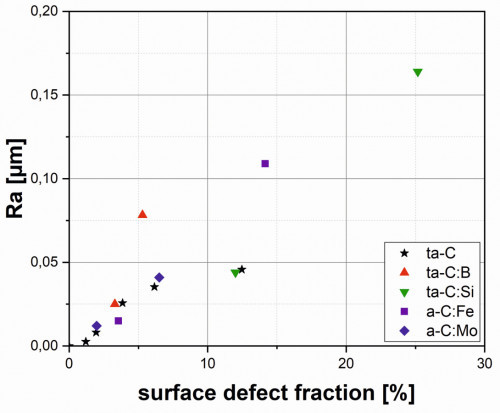 Fig. 7: Ra values as a function of the surface defect fraction for the different doping systems The high defect fraction in pure ta-C coatings can thus be explained by the fact that by far the greatest amount of growth defects are present on the surface as well as by the formation of very big defects. This suggests that the emission rate of initial particles from undoped carbon cathodes is particularly high, leading to the formation of a great amount of new growth defects when incorporated into the growing film. In all cases of doped cathodes, a lower number of growth defects was detected on the surface in respect to pure ta-C coatings. Doping graphite cathodes with the selected elements hence results in a lower emission of initial particles and thus to a lower surface defect fraction. The origin of this effect could be explained by different evaporation behavior of doped carbon cathodes. The emission rate of particles very much depends on the surface properties, density and electrical conductivity of the cathode material [3, 15, 28]. Hence, by changing the cathodes microstructure and chemical composition the number and size of particles emitted can be influenced. Concerning doped (t)a-C:X coatings (Fig. 6) a low surface defect fraction at ta-C:B and a-C:Mo coatings can be detected. However, it can be observed that on the one hand significantly more surface defects are formed in ta-C:B coatings than with the other dopants, but on the other hand this leads to a low surface defect fraction. This in turn indicates a high number of very small emitted initial particles and grown defects at ta-C:B, whereas for a-C:Mo a small amount of defects with a comparable higher area is formed.
Additional topographical information about the surface properties of the doped and undoped coatings were provided by the Ra values from tactile profilometry. Ra values of the different coatings are shown as a function of the surface defect fraction in Figure 7. It can be clearly seen, that the roughness is increased with increasing surface defect fraction. A comparable high increase of the roughness with the surface defect fraction is observed for ta-C:Si and a-C:Fe. The curve for ta-C:B is of interest, showing comparable weak increase of the surface defect fraction with the coating thickness as shown in Figure 5, but a steep increase of the roughness with the surface defect fraction. For a better understanding of the correlation of the roughness and the surface defect fraction a finer resolution of the measured values is necessary.
Conclusion
This work showed the influence of dopants on the coating properties and on the formation of surface defects. Detailed investigations were performed using laser arc evaporation of graphite and graphite composite targets to investigate the influence of the doping on the coating properties, in particular on the surface defect fraction.
Dopants X=B, Si, Fe and Mo were used to compare the properties of the resulting (t)a-C:X coatings with pure ta-C. Results showed that the non-metallic dopants (B, Si) produced hard, ta-C-like coatings, while the metallic dopants (Fe, Mo) caused rather softer, graphitic a-C-based coatings.
The study focused on evaluating coating surfaces with respect to the surface defect fraction caused by arc-induced particles. For these analyses, a surface characterization method was developed based on the automatic evaluation of light microscopy images, which is hallmarked by the following approaches:
- LM image acquisition allows a uniform and repeatable illumination at a constant magnification of 500x
- Digital image processing with Image J enables automatable implementation, repeatable image post-processing and correction.
By evaluating the surface coverage with defects, a so called defect fraction was defined. The following correlations were found:
- Accuracy of the method is limited by a surface defect fraction of around 40 %
- The surface defect fraction of the doped (t)a-C:X-coatings is lower than observed on pure ta-C
- B- and Mo-doped carbon coatings are the smoothest coatings with lowest surface defect fraction.
The method of optical surface evaluation with determination of the surface defect fraction is a reliable method for determining the particle-induced defect density in arc-deposited carbon films. It correlates well with the classical topographic roughness measurement. In contrast to the tactile measurement, however, the optical method described captures a significantly larger area fraction and is thus more reliable.
Further research should be conducted on:
- Understanding of the growth mechanism of defects in ta-C and doped carbon coatings and their dependency from deposition process parameters
- Investigations of the evaporation mechanism of pure and composite graphite targets
- Influence of the content of dopants on the coating properties.
Acknowledgement
to the colleagues and students of the Department of Carbon Coatings at Fraunhofer IWS and Dr. Jörg Kaspar and M.Sc. Martin Kuczyk, members of the Group of Materials and Failure Analysis.
Literatur
[1] W.I. Milne: Tetrahedrally bonded amorphous carbon, Journal of Non-Crystalline Solids, 198–200, 1996, 605–610
[2] C. Schulze: Laserpulsabscheidung (PLD) und Laserpulsspannungsrelaxation (PLS) von ta-C–Schichten und Untersuchung des Einflusses von Dotierungskonzentrationen auf die Schichteigenschaften, Diplomarbeit, 2011
[3] B. Schultrich: Tetrahedrally Bonded Amorphous Carbon Films I, Springer, Berlin, Heidelberg, 2018, Online, Available: https:// doi.org / 10.1007/ 978- 3- 662- 55927- 7
[4] J. Robertson: Diamond-like amorphous carbon, Materials Science and Engineering, R 37 (2002) 129–281
[5] M. Chhowalla; Y. Yin, G.A.J. Amaratunga; D.R. McKenzie; T. Frauenheim: Highly tetrahedral amorphous arbon films with low stress, Appl. Phys. Lett., vol. 69 (1996) no. 16, 2344–2346, doi: 10.1063/1.117519
[6] M. Chhowalla; Y. Yin; G.A.J. Amaratunga; D.R. McKenzie; T. Frauenheim: Boronated tetrahedral amorphous carbon (ta-C:B), Diamond and Related Materials, vol. 6 (1997) 207–211
[7] W. Dai; X. Gao; J. Liu; Q. Wang: Microstructure, mechanical property and thermal stability of diamond-like carbon coatings with Al, Cr and Si multi-doping, Diamond and Related Materials, vol. 70 (2016) 98–104, doi: 10.1016/j.diamond.2016.10.017
[8] J.-I. Kim; Y.-J. Jang; J. Kim; J. Kim: Effects of silicon doping on low-friction and high-hardness diamond-like carbon coating via filtered cathodic vacuum arc deposition, Scientific reports, vol. 11, (2021) no. 1, 3529, doi: 10.1038/s41598-021-83158-4
[9] X. Li; D. Zhang; K.-R. Lee; A. Wang: Effect of metal doping on structural characteristics of amorphous carbon system: A first-principles study, Thin Solid Films, vol. 607 (2016), 67–72, doi: 10.1016/j.tsf.2016.04.004
[10] S.C. Ray; W.F. Pong; P. Papakonstantinou: Iron, nitrogen and silicon doped diamond like carbon (DLC) thin films: A comparative study, Thin Solid Films, vol. 610 (2016), 42–47, doi: 10.1016/j.tsf.2016.04.048
[11] J.S. Chen et al.: Deposition of iron containing amorphous carbon films by filtered cathodic vacuum arc technique
[12] N. Pasaja; S. Sansongsiri; S. Intarasiri; T. Vilaithong; A. Anders: Mo-containing ta-C deposited by dual filtered cathodic vacuum arc with nselective pulsed bias voltage, Nuclear Instr. Methods Phys. Res., B 259 (2007), 867–870, doi: 10.1016/j.nimb.2007.02.093
[13] P. Panjan; A. Drnovšek; P. Gselman; M. Čekada; M. Panjan: Review of Growth Defects in Thin Films Prepared by PVD Techniques, Coatings, vol. 10 (2020) no. 5, 447, doi: 10.3390/coatings10050447
[14] S. Kumar; D.K. Aswal: Recent Advances in Thin Films, Springer, Singapore, 2020
[15] A. Anders: Cathodic Arcs: From Fractal Spots to Energetic Condensation, Springer, New York, 2008
[16] Fraunhofer-Gesellschaft: Verfahren zur Bearbeitung von Oberflächen einer Beschichtung aus hartem Kohlenstoff, DE102006010916A1
[17] F. Kaulfuss et al.: Effect of Energy and Temperature on Tetrahedral Amorphous Carbon Coatings Deposited by Filtered Laser-Arc, Materials, vol. 14 (2021) no. 9, Basel, CH
[18] D. Drescher; J. Koskinen; H.-J. Scheibe; A. Mensch: A model for particle growth in arc deposited armophous carbon films, Diamond and Related Materials, vol. 7 (1998), 1375–1380
[19] D. Drescher; A. Kolitsch; A. Mensch; H.-J. Scheibe: Investigation of surface topography, morphology and structure of hard amorphous carbon films by AFM and TEM, Fresenius Journal of Analytical Chemistry, vol. 353, (1995), 690–694
[20] M. Polster: Abscheidung von dotierten Kohlenstoffschichten mit dem laserinduzierten Vakuumbogen, Diplomarbeit, 2002
[21] M. Kandah; J.-L. Meunier: Study of microdroplet generation from vacuum arcs on graphite cathodes, J. Vac. Sci. Technol. A, vol. 13, 1995 no. 5, 2444–2450
[22] L. Lorenz; T. Chudoba; S. Makowski; M. Zawischa; F. Schaller; V. Weihnacht: Indentation Modulus Extrapolation and Thickness Estimation of ta-C Coatings from Nanoindentation, J. Mater. Sci., accepted
[23] Image J: Image Processing and Analysis in Java, Online, Available: https://imagej.nih.gov/ij/
[24] B. Jähne: Digitale Bildverarbeitung und Bildgewinnung, 7th ed. Springer, Berlin, Heidelberg, 2012, Online, Available: http:// dx.doi.org / 10.1007/ 978-3-642-04952-1
[25] A. Erhardt: Einführung in die Digitale Bildverarbeitung: Grundlagen, Systeme und Anwendungen, Vieweg+Teubner / GWV Fachverlage GmbH, Wiesbaden, 2008, Online, Available: http:// dx.doi.org /10.1007/978-3-8348-9518-9
[26] L. Priese: Computer Vision: Einführung in die Verarbeitung und Analyse digitaler Bilder, Springer Vieweg, Berlin, Heidelberg, 2015, Online, Available: http://dx.doi.org/10.1007/978-3- 662-45129-8
[27] Darstellung der Ergebnisse von Partikelgrößenanalysen: Teil 1: Grafische Darstellung (ISO 9276-1:1998), 9276-1, DIN ISO, 2004
[28] J.E. Daalder: Components of cathode erosion in vacuum arcs, J. Phys. D, vol. 9 (1976), 2379–2397
[29] T.F. Zhang; Z.X. Wan; J.C. Ding; S. Zhang; Q.M. Wang; K. H. Kim: Microstructure and high-temperature tribological properties of Si-doped hydrogenated diamond-like carbon films, Applied Surface Science, vol. 435 (2018), 963–973, doi: 10.1016/j.apsusc.2017.11.194
[30] L.L. Wang et al.: Structure and properties of Mo-containing diamond-like carbon films produced by ion source assisted cathodic arc ion-plating, Applied Surface Science, vol. 286 (2013), 109–114, doi: 10.1016/j.apsusc. 2013.09.029
[31] C.P. Klages; R. Memming: Microstructure and Physical Properties of Metal-Containing Hydrogenated Carbon Films, MSF, 52-53, 1991, 609–644, doi: 10.4028/www.scientific.net/MSF.52-53.609
[32] M. Chhowalla; Y. Yin; G.A.J. Amaratunga; D.R. McKenzie; T. Frauenheim: Boronated tetrahedral amorphous carbon (ta-C:B), Diamond and Related Materials, vol. 6, 1997, 207–211


